






Getting Started
Introduction
This Getting Started should help you to determine the best way to manage your System on Chip ("SoC") design project. One of the aims of SoC Labs is to bring industry best practice to academic led projects.
We achieve this by encouraging the following design mentalities:
- Maintain a clear Project Management plan based on well established design flow steps
- Maximising reuse of pre-verified reference designs to allow maximum effort on your unique custom IP
- Using a structured verification flow, enabling re-use in validation steps at each stage of the design process, from architectural investigation to silicon die bring up.
We have developed this design flow guidance and the milestone tracker in SoC Labs projects to be a checklist for activities you should consider, follow and record your work and progress against that should lead to a successful SoC Labs project.
Project Management
Project Management is key to successful projects. It is something industry teams invest time and discipline in working through and is often not undertaken in such a way in academic projects, especially in small teams or individuals. Project Management does not need to be seen as a burden in small projects as the time and discipline should be relative to the size of the project.
This site provides a simple framework of design flow guidance aligned to milestones for you to record and track your progress as an industry project would. You should use your milestones in your project to make notes and record progress and this will help you maintain a clear Project Management plan throughout the project. Academics often find it hard to estimate how long tasks will take. That is because they do not have the experience or have not recorded how much these tasks took in past projects, industry seems to better retain this knowledge. By recording and sharing both your estimates and actual here in SoC Labs you help maintain a pool of shared experience. You can develop your own estimates for target completion dates for milestones based on other SoC Labs projects. You can also use your own milestone progress to gauge future work.
Beyond maintaining the key milestones of the project tracker, it is important that team members (or yourself if this is a single person project) keep track of the many small tasks that are needed and outstanding. We recommend either using any tools within your source repository such as Git, or set up an issue tracking system such as Jira. All good industry project use such tools.
Project Meetings
There are a number of types of meetings that teams have in industry. For example, Design Reviews, Stage completion, etc. If working in a team it is important to schedule frequent Project Status Meetings to ensure everyone has a consistent view of the project.
Project Development Processes
Over many years industry has developed a small number of different project / design processes or methodologies. Our view at SoCLabs is not to be proscriptive, apart from there should be an active decision by you to adopt one and make best use of it for the specific design activity.
The two extreme variations of these methodologies are Agile and Waterfall.
Waterfall
Waterfall is best used when the project scope and specification are very well defined in advance and the work can be broken down in phases of work that are simple decompositions of the previous design task without too much need to re-confirm the understanding of the project scope.
Agile
Agile is best used when the project scope and specification is not clearly defined and has to be developed along with users of the eventual silicon as the project progresses. Rather than a series of decompositions the work is a series of iterations, the first being the Minimal Viable Product that can be used with the users to get them to express their needs more thoroughly.
SoC Design methodology
In practice, a project sits somewhere between these two extremes and you actually use both approaches in different aspects of a full SoC design. For example a well defined finite state machine can very simply be developed using a more waterfall based approach via simple decompositions. In the Physical Design stage, agile iterations may be needed to adjust the trade off for different demands of Power use, Performance or Area cost as these may not be fixed at the project start but found by agile iteration and discussion with users or project supervisors.
Structure within your Project
There are a small number of important structures to maintain in your SoC design project and they are often hierarchical organisation schemes. For example the guidance in this SoC Labs design flow has a hierarchical organisation scheme. How the various IP parts of the SOC system design are separated and laid out usually follow a hierarchical organisation scheme. How the various files in a project source control repository are structured is a hierarchical organisation scheme. We will come back to these at various points in the design flow guides.
Development environment
It is important to have a consistent development environment across your team. This comes down to two real areas of focus. Your physical environment - EDA tooling, FPGA boards, operating system, compute system so that everyone is working in a consistent environment to minimise problems and increase reproducability.
The second consideration of the management of your deliverables and work. This focuses on the code you are working on, documents you are creating and project management tools you are using. You need a good way to communicate across your team, whether that be through slack and teams and need traceability of ideas.
Version Control and Deliverable Management
Version Control systems, such as Git, are incredibly useful tools and help provide structure to project work and design activities. These are in widespread us in industry and are a pre-requisite for a well managed project and enables:
Collaboration with people able to work on different features of a project independently using branches which can then be merged, making it easy to track and visualise changes as well as see who is contributing to specific parts of a project
Delivery to others by download and use your code by cloning the repositories
They also provide a clear development history, manage and merge parallel work streams and help bisect and trace back the introduction of bugs within a system which is incredibly valuable, especially in large projects. They afford the following features:
- Work trees. Allow you to work on two separate work items on a single repo without needing to recheckout the repository.
- Branch management. Having feature, fix and release branches can help with project management. Please click here for more detail on branching strategies.
- Submoduling. This is very valuable in SoC Labs focused work. We have structured our repositories in a way where they can be submoduled in to a project and be used as modular building blocks for your project. We would encourage using the same structure for your own components such as accelerators. We provide technology, tools and flow repos as well as SoC repos which are all modular and often stacked to accomplish specific work and encourage reuse so not everything needs to be developed from the ground up.
- Tags and Releases. Tagging can be really useful to create snapshots at fixed points in time for milestones. This is helpful if something breaks on a branch in future, you can roll back to a known point in time. Using this alongside releases gives you something you can project outside of your team that you are confident in its stability.
- Artifact Management. You can attach artifacts - things that are generated from your source code in your repository that aren't checked in from a fixed point in time. This saves the repository being cloned and ran to build these deliverables. Other tools such as artifactory achieve a similar task but Github has a more accessible version built in.
- CI/CD. Gitlab and Github both have CI runners. This removes the need of having to manually run all of your flows. You can get these pipelines to run automatically which can be great to quickly pick up on bugs that if been introduced in recent code commits.
Project Structuring
Relating back to the point of submoduling within Git, it is important to consider how you want to structure you project so it is logical and easy to navigate. You want clear separation between source code for different parts of the project so you are able to go and make modifications to specific parts of the repository which don't conflict. This becomes increasingly important when you are working with multiple people on separate development branches as merge conflicts can be a nightmare to resolve.
Having separation between your source RTL, wrapper RTL for you specific implementations, flows and constraints for different technologies, clean separation between your Golden Reference Model, usually a Python Model in the architecture we are suggesting, and your verification environment and testing is important. It is worth spending some time as a team to consider how you will separate this out, will you have multiple submodules for different engineers working on verification, design and modelling or do you want to do it all in one repository. Having a clear strategy ahead of time that everyone is in agreement on and everyone knows their domain can reduce stress down the line. Building common building blocks and work flows, for example, everyone using the same simulation flow, simulator and testbench rather than everyone building their own can make maintenance a lot simpler.
These principles should be repeated in the way code is structured too.
- nanoSoC reference design
NanoSoC is designed to support projects with custom acceleration hardware where the SoC architecture between projects is more-or-less consistent. The top-level project is a wrapper around both the SoC Labs reference SoC design as well as a repository containing the custom accelerator. Forking the soclabs/accelerator-project allows you to use that as a baseline to build your own project around NanoSoC. This will involve submoduling your own custom accelerator repository and then attaching that in to the accelerator expansion region of the SoC. The project template also contains flows for synthesis and verification which can be used across the custom project. The top-level system repository contains system wiring and verification material for the nanoSoC reusable design IP soclabs/nanosoc_tech
It is worth reading project structure flow to get an idea of the suggested project structure.
The NanoSoC Tech IP repository contains the core SoC structural IP but not the IP provided via the Arm Academic Access Program (or from other IP licensing routes). The repository structure adopted for the NanoSoC reference design keeps all Arm IP in a non-checked in environment for security. These IPs are downloaded and stored on a filestore, and then the flow reference the location of these files using environment variables.
See the latest nanoSoC reference design for details. Please read the README file for the git resources.
A deep-dive in to project structuring and the rationale behind why we have structured our reference projects in such a way is explained in detail here.
External dependencies
It is important to version lock external dependencies when in development. Pick a version of your tools and external IP and stick with it. This doesn't mean don't roll forward if you need to but don't roll forward for the sake of it as it can cause headaches as unexpected problems with compatibility or bugs may be introduced setting you back. Keep up to date with new IP versioning, looking at the change logs provided alongside the IP but especially when getting close to tapeout, getting to a point where your RTL is frozen and your tool versions are stable is important as you really want to minimise risk at this stage.
Operating-system Environment
A large amount of SoC Labs reference designs use environment variables to allow for flexibilitiy and portability across projects and development servers. The simplest way to enable this, where multiple projects may be inflight on a compute system at the same time, is to use set_env scripts. Sourcing these scripts modifies you environment variables across your work environment and creates relative paths to the root of your project and to the tools within. Building upon this methodology within a project is very much encouraged.
Project Readme
It is always important to have a quick getting started Readme for your project repository. This will usually render on your Git provider and tells people how to clone the project and run some basic flows. It is helpful to give an introduction to the project, the goals and the work that has been done and reference external work. You can always add a link to your SoC Labs project. This helps other people to quickly and easily understand your project.
IP Access
The SoC Labs reference designs are built around core Arm IP components. License agreement sometimes need to be signed to get hold of this IP. Arm supports the semiconductor industry by providing highly re-usable IP for the compute sub-system needed within a SoC design. This significantly simplifies the system development process. SoC Labs as a community uses projects to help us share and reuse hardware and software developments around core Arm IP to enable us to better achieve our research goals. A SoC Labs project is likely a selection and configuration of Arm IP to define the core of the system architecture with additional specific blocks developed uniquely as part of a project. Arm provide under the Arm Academic Access programme much of their IP to researchers for academic purposes for no charge. Its free to sign up, please ensure that you have joined the programme here.
You will need to obtain permissions and download some of the Arm IP which is listed in the technology section of this SoC Labs site. The SoC Labs reference designs extend and enhance the core Arm IP tailoring it for easy adoption by the academic community. One of the first steps in Architectural Design is IP selection. which outlines some of the IP you may need to create your System on Chip.
It is worth keeping this IP downloaded in a common area but restricted through file permissions so only people who have registered to AAA programme can gain access to these files.
Downloading open-source IP which is not version controlled in a system like Git, such as files you might access from opencores, is advisable to maintain a similar structure as to the proprietary IP so that everyone in your team has access to exactly the same files.
- nanoSoC reference design
The nanoSoC reference design can utilise DMA controllers to manage the transfer of data to and from any custom accelerator. These DMA controllers need to be obtained from Arm. There are two levels of access in Arm Academic Access; the basic Foundation level and the Mainstream level. The DMA controllers are in the Mainstream level which is not the default AAA subscription. You may need to request an upgrade of your AAA subscription from Foundation level to the Mainstream level to make best use of the nanoSoC reference design.
EDA Tool selection
EDA Tool vendors have made different choices on how to implement specific steps in each of the high level design flow stages with variations in some file forms and even subtle differences in how language constructs are implemented. This means that a design that will pass verification in one tool chain may not pass verification in another tool chain. Additionally their are significant variations in warning messages across tool chains.
There are many reasons you might select a specific vendor toolset:
- What licenses are available to you within your institution
- What level of support , expertise and knowledege of those in your institution
- Some georestrictions apply to specific EDA tools
Some tools, such as Verilator work, in different ways to commercial EDA tools. Depending on what you are trying to achieve, it can sometimes be worth using different tools doing the same job, such as simulation, if you are license limited or need to have faster simulations at the expense of less debug visibility.
Using tools such as modulefiles (Environment Modules) can be a really clean and simple way to manage different versions of EDA tools and set up environment variables. Please read more about this here if you would like to set this up.
The methods to utilise the EDA tool options and differences will be explained in sections for each tool within each generic design flow stage.
- Cadence
Information on the Cadence design flow tools.
We encourage the community to share more examples throughout this design flow part of the site, adding material and discussions on such tools and example flows. You can log in and edit the pages to add material that will be moderated or simply add a comment below.
Design, Verification and Validation
Designing your custom SoC is only half the work that needs to be done. It is always important to reflect back to you specification to ensure that what you have build not only works but also actually does what you set out to do.
Verification is often stated as "does the design work and does it pass all the tests?". Validation is often forgotten. This focuses on "does the design actually do what it needs to?". This involves creating a validation test plans based on all of the features and requirements laid out in the overall project specification, whether that is stated at the start in a Waterfall approach or developed over time in an Agile approach. Having a complete specification of the project ensures you are actually building a solution to the problem you set out to solve.
And additional methodology to adopt is Design for Test, making sure what you are building is actually testable, how can you test it and how easy is it to debug?
At SoC Labs we are encouraging the concept of verification reuse. A lot of the effort can be put in upfront in establishing the best framework for verification and validation at the Architectural and Behavioural stages such that for a Design under Test the same tests and resources can be used throughout the design process flow stages all the way through to post silicon bring up. Our ail is to ensure there is consistency throughout project development and features and criteria don't fall through the net the further the project development progresses and time becomes more pressing. SoC Labs aims to provide a baseline level of SoC verification based on our reference SoCs which can then be used as the core infrastructure for you project specific testing.
Having an explicit and thorough verification and validation strategy is something industry invests in and is also key to project success. Finding bugs and gaps early can save both time as well as large amounts of stress and money as bug fixing becomes significantly more costly the closer you get to tape out as many steps need to be revisited.
See Verification Methodology for more details.
Project Design Phases
This design flow area of the SoC Labs site sets out the phases involved in an ASIC SoC design activity going from project conception to having a validated silicon system. FPGA activities will take a subset of these phases but it is equally important that the whole flow is read and becomes familiar. Please read through these design flow pages to get a high-level understanding of each phase before digging deeper in to each one of the sections within the website tree.
From a high-level, these phases are:
- Architectural Exploration and Specification
- Behavioural Design
- Logical Synthesis
- Physical Implementation
- Post-silicon bringup and testing
Creating your SoC Labs Project
SoC Labs projects provides a simple way to document and mananage the activities needed to take a SoC design from initial concept to fabrication and post silicon validation.
The is done within a SoC Labs project on this site, you can see many examples here. Getting started is very simple, you need just a project description and preferably an image that represents the project.
Initial Project Description
The initial project page should lay out your project aims and what you are hoping to accomplish. Initially is a short description to help us support you and also for the community to understand if there are common tasks that could be shared. Building out the rest of the activities on the project can be done over time. You can always edit and add new details as you go.
Project image and other images
Though not mandated, having a clear block-diagram of your system or visual representation of your project outcome can be helpful for others when looking at projects.
Within project text we try to use diagrams, waveforms and tables to help explain concepts and projects and it is advised that you do this also when writing about your project. Keeping it clear, using tools like draw.io and adding structure can be a great way to refine your presentation of your project. Capturing screenshots from EDA tools, such as block diagram implementations from Vivado, or layouts from Place and Route tools can be valuable to show others what they will be encoutering as they go through the process of producing a project.
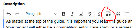
These can be added using the upload image in the editor toolbar.
Lets get started...
Simple follow this link to create your SoC Labs project
Tracking Progress
Once created it is easy to track progress by simply adding each of the activities needed to complete the project, simply 'Add new project milestone' and ...

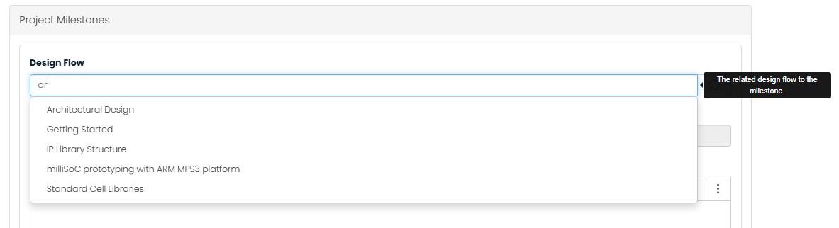
and then select the design flow step by starting to type and select from the drop down list.
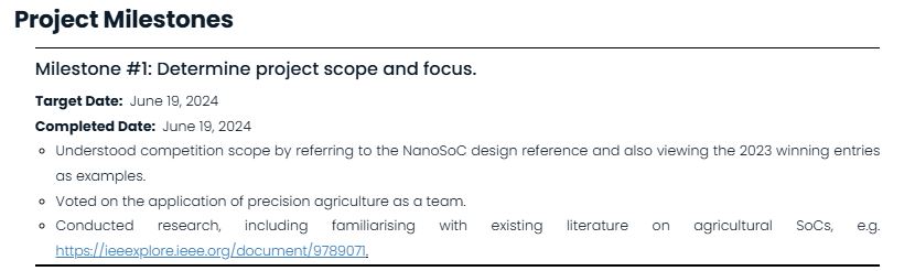
When you complete a step you can capture the date and details of the work so you can review as and when needed. It also provides help to other SoC Labs projects who can use the information to aid their projects. Here is an example from the Sensing for Precision Agriculture project by the University of Sydney.
Each of the stages and steps in the design flow area has generic information for the activity and additional information in relation to each of the SoC Labs reference designs. These reference flows reflect back how each design flow step was accomplished with more specifics regarding that reference design.
Adding your first Milestone
At any time you can add your first Milestone. This can be either a free from milestone of your own
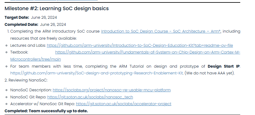
You can previous work relating to this project, or training you or the team need.
or a milestone for this Getting Started activity.
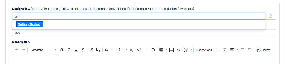
Here you can add statements that reflect on all of the points made in the Getting Started guide, especially project management, your design methods, links to your development environment if they are in the public domain on say Git, etc. Start to think about the points raised in this guide, they are not exhaustive but are listed to give a starting point as a point of inspiration.
- Choice of Version Control system
- How your project will be initially structured
- ...
Don't forget to give some estimates of timeframe for activities and come back and give actuals when you complete each milestone.
Conclusion
This Getting Started guide should provide you with an overview of how to get started with a System-On-Chip Project. Many decades of industry SoC design projects has shown that time invested in establishing the right development environment, following appropriate design and verification methods and tracking and documenting project status and progress lead to successful project outcomes. We have tried to make this process simple by giving you a baseline of reusable assets. Success will depend on your effort and discipline in using them but we are here to help and can best do that if you submit project milestones such we can help you.
We look forward to taking your project through to a successful outcome.
If you have any questions or would like to offer any views or additional information then please provide any comments or points below.
Projects Using This Design Flow

Experts and Interested People
Members




Related Project Milestones
| Project | Name | Target Date | Completed Date | Description |
|---|---|---|---|---|
| Arrhythmia Analysis Accelerator : A-Cube | Getting Started (175) |
Implement and test the Soclab encryption example in the ZCU104 FPGA board. |
||
| Sensing for Precision Agriculture | Getting Started (175) |
Milestone #1: Determine project scope and focus.
|
||
| Sensing for Precision Agriculture | Getting Started (175) |
|
||
| Use of the Synopsys HAPS® FPGA-based prototyping environment | Getting Started (175) |
The guidance for the Getting Started milestone states it should help determine the best way to manage the project and to provides a simple way to manage the activities to be completed. Project Management: This project is not a System on Chip activity that follows the normal path of design flow steps. This project will selectively use some of the design flow steps and add some free form milestones as a way to guide the project to meet target dates to better drive the project to completion. As milestones are completed the date and details of the work need to be captured. Design Method: The project will use an agile method, with short development cycles, this will allow user needs to be established and then delivered. Agile usually defines a first iteration as a Minimal Viable Product. Access to IP: There are two aspects to this project:
Synopsys IP: SoC design IP: Version Control: Until a better alternative can be identified any materials developed by this project should be held in the SoC Labs git repository. Project Structure: This will need to be defined in more detail as we understand the use cases and information and other assets that need to be developed as part of the project. The initial known outputs are:
Verification Methodology: As outlined part of the project is to follow a typical SoC Labs reference design flow deployment using the HAPS to allow the three major uses of FPGA prototyping environments:
Both MVP deliverables are defined and the first exists. The community knowledge base is the HAPS-SX Development space on the SoC Labs Confluence (getting started, network and command-line configuration, adding a board, HOSTIO and OpenOCD debug, ConfPro-SX on WSL, DDR memtest runbook). The course has not been started. |
||
| AHB eXcecute in Place (XiP) QSPI | Getting Started (175) |
Setup environment for the AHB QSPI IP |
Add new comment
To post a comment on this article, please log in to your account. New users can create an account.