View Reference Design Projects
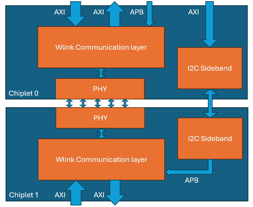
For a chiplet system, you need a communication interface between chiplets. The industry has developed standards that require complicated IPs around UCIe and the CHI interface from Arm. For many academic projects these are probably more complicated than needed . The aim of this project is to produce a simple chiplet communications interface based around the open standard AXI protocol.
The project is hosted here: https://git.soton.ac.uk/soclabs/chiplets/axi-chiplet-controller
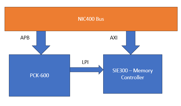
The PCK600 Arm IP provides components to allow a power control infrastructure to be distributed in a SoC in order to make a design energy efficient. Arm provide the IP as part of their Power Control System Architecture that can be used to control the power states of various parts of the system. This control of the power infrastructure is achieved through the use of the Power Policy Unit (PPU). This unit has an APB interface to allow for software control, and some low power interfaces that can connect to the power controllable IP within the system.
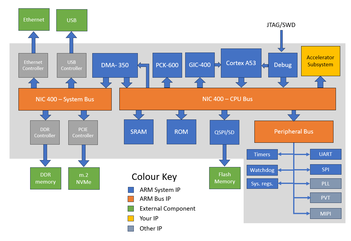
megasoc has been designed to provide a complex SoC component that can 'host' and support the development and evaluation of research components or subsystems. The design allows for seamless transition from FPGA to physical silicon implementation via a pre-verified programmable control system that allows reuse of software and diagnostic functionality to facilitate the configuration, control and diagnostic analysis of research hardware such as custom accelerators or signal processing.
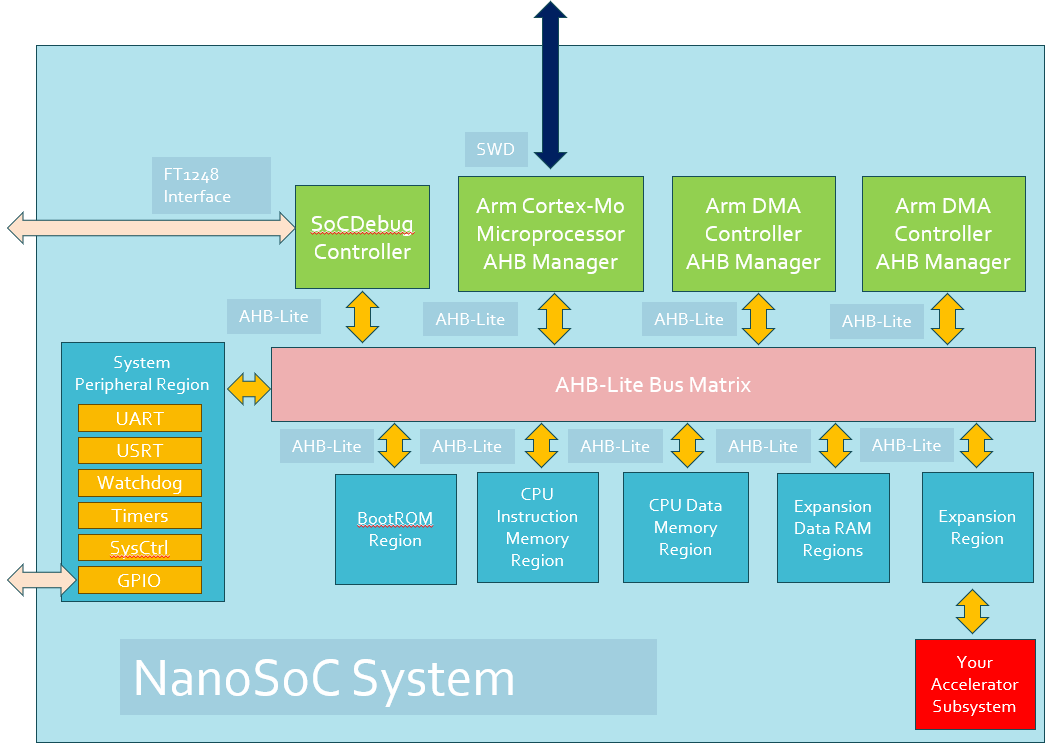
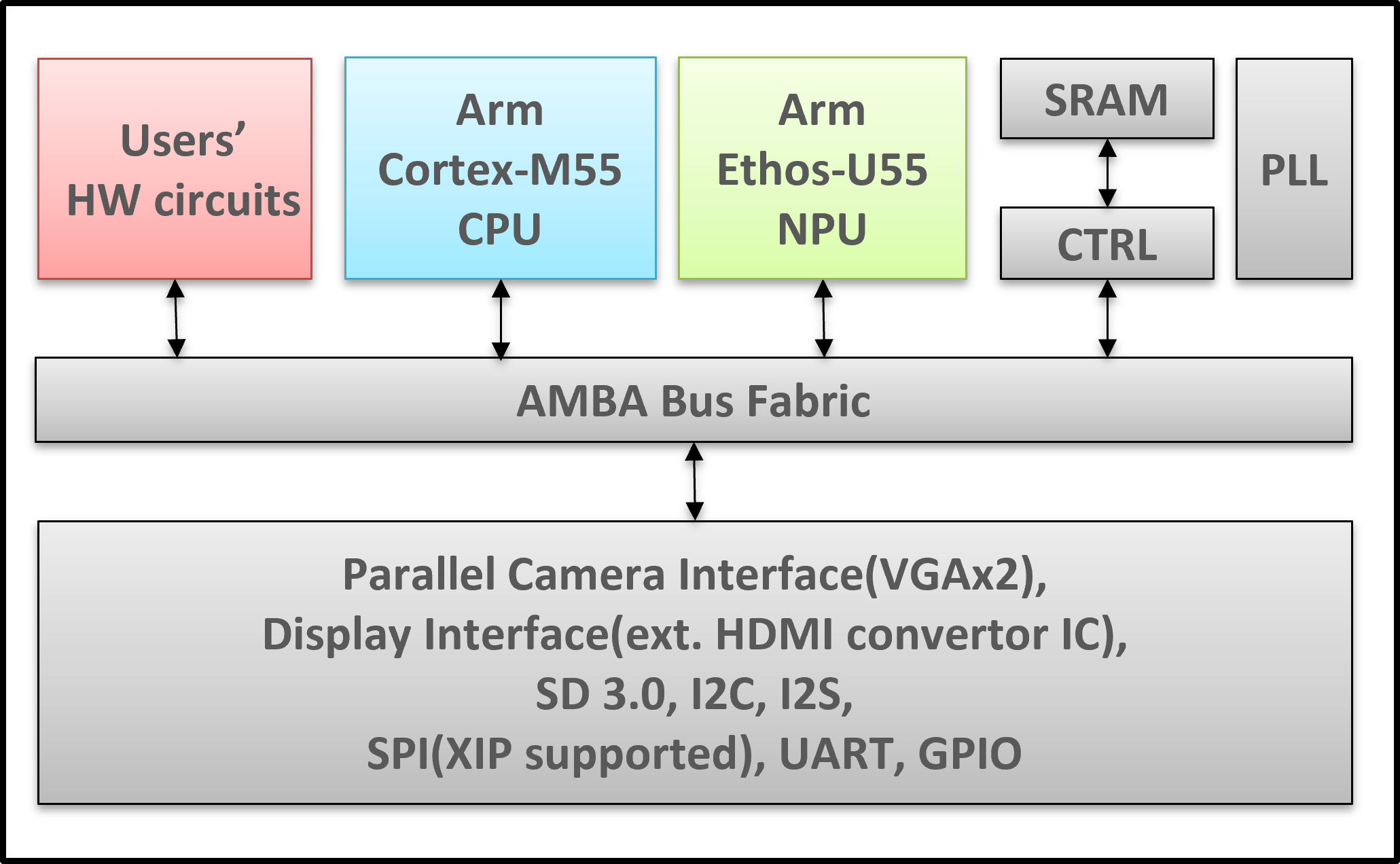
The Arm Cortex-M55 AIoT SoC design platform is an AIoT subsystem that allows custom SoC designers to integrate their hardware circuits and embedded software for differentiation. The platform is developed by TSRI (Taiwan Semiconductor Research Institute) to support academic research on SoC design. It's built on the Arm Corstone-300 reference package, featuring the Cortex-M55 CPU and Ethos-U55 NPU.
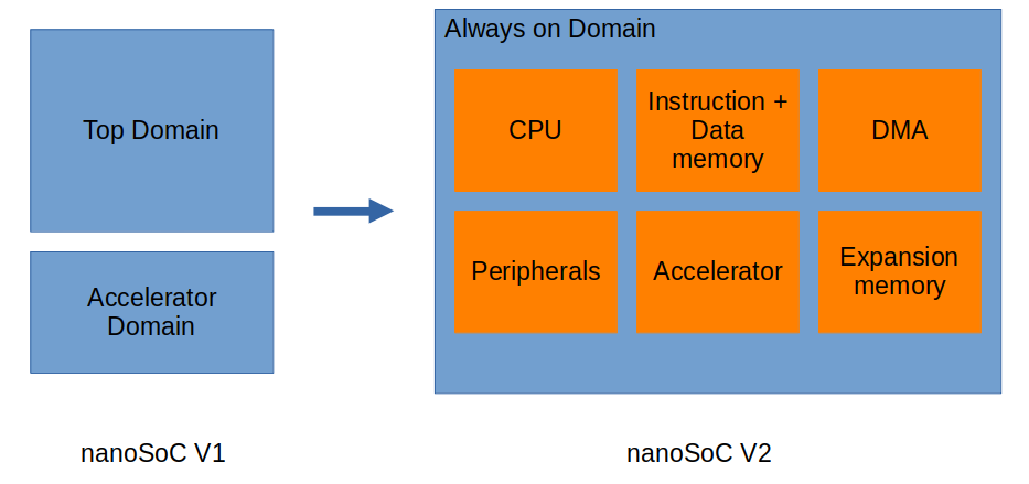
As part of plans for continued development of nanoSoC one area that requires improvement is the power structure of system. The first iteration of nanoSoC contained 2 power domains: the accelerator domain and the remainder of the SoC. Both power domains were connected to external pins to allow connection to separate external voltage regulators and power measurement ICs, as implemented in the first version of the nanoSoC testboard.
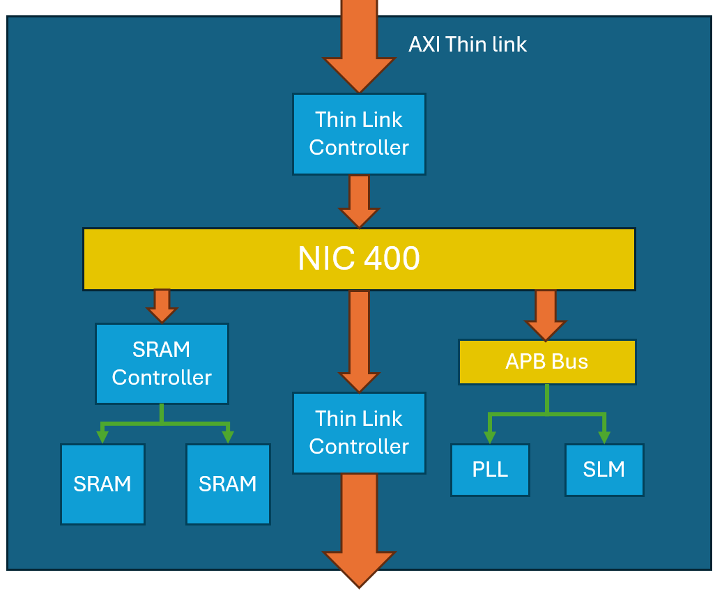
On-chip SRAM in ASICs can use a significant area, which equates to a significant cost. One solution is to make the memory off-chip. This project explores the use of Arm IP to create an SRAM chiplet design. The benefit is that standard memory chiplets can be fabricated at lower cost and used across multiple projects, miminising silicon area to the unique project needs.
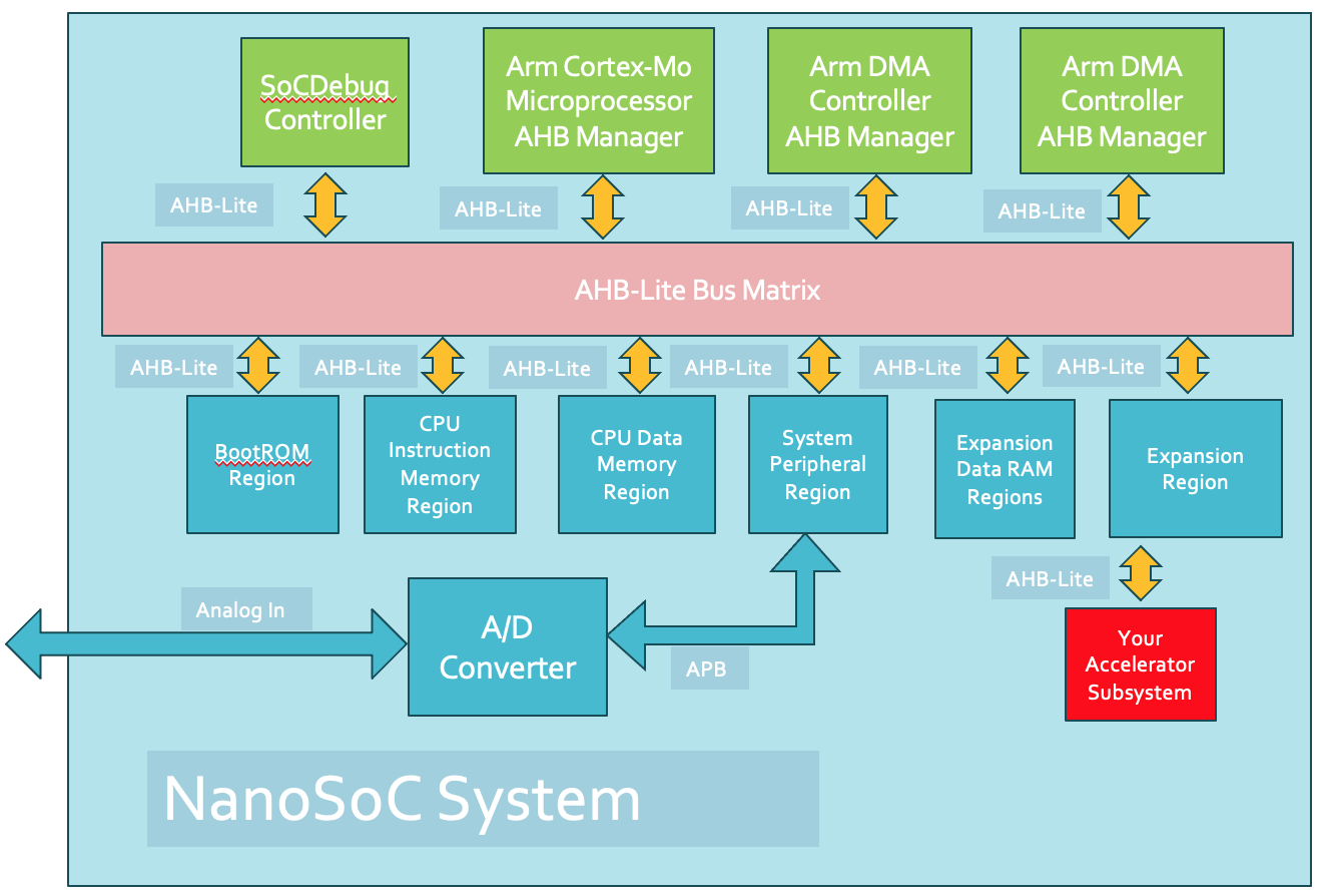
The aim of this project is to define a mixed signal subsystem for the nanosoc reference design.
The mixed signal subsystem should be able to sample analog signals at a regular sampling rate, and transmit a digital representation of this signal to the rest of the nanosoc system. In order to interface with real-world signals in a digital System on Chip ("SoC"), an analog to digital conversion ("ADC") is needed.

 David Mapstone
 Daniel Newbrook
 David Flynn