AHB eXcecute in Place (XiP) QSPI
The instruction memory in the first tape out of nanosoc was implemented using SRAM. The benefit was the read bandwidth from this memory was very fast, the downside was on a power-on-reset, all the code was erased as SRAM is volatile memory. An alternative use of non-volatile memory would benefit applications where deployment of the ASIC does not allow, or simply time is not available for programming the SRAM after every power up.
Non-volatile memory ("NVM") comes in different forms, but for microcontrollers the most typical type of NVM is flash. In industrial scale tape outs, companies may opt for on chip flash, as the area cost of adding this is typically recovered in selling large volumes of chips. For academic tape outs, the area needed for flash can be costly. The alternative is off-chip flash. There are really 2 categories, parallel and serial. As expected, parallel flash can give higher bandwidth at the cost of extra pins, and serial flash offers lower bandwidth but with significantly fewer pins.
For nanosoc and other small scale SoCs, it makes sense to opt for the serial flash as the ASIC implementation area of nanosoc has previously been I/O constrained (i.e the area of the die is small and impacts how many pins can fit on the die edge). For serial flash, SPI is the most common interface, and is often extended to dual, quad or octal SPI (adding extra data I/O pins). This project has opted for a QSPI implementation as this provides the good bandwidth/no. of pins option. The project may later extend the IP to support dual and octal SPI.
A lot of flash chips implement eXecute in Place (XiP). This feature means that for consecutive reads, you can omit sending the command byte, and just send the address. This can slightly increase the bandwidth of the flash accesses. For XiP it also makes sense to use a fully memory mapped interface, with an associated cache.
The code for this project can be found on our Git here.
Architectural Design
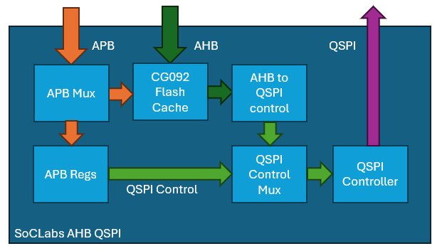
The fundamental design for the architecture is as below:

CG092 Flash Cache
The CG092 flash cache is a cache provided by Arm. It is instantiated between the bus interconnect and the flash controller to support caching. It has been optimised for fetching and caching instructions for M-class processors (particularly M3 and M4). The cache controller has a 32-bit AHB-lite subordinate that connects to the SoC bus, and a 128-bit AHB-lite manager that is connected to the "AHB to QSPI control block". The CG092 also requires an APB port for configuration of the cache controller
APB Mux
A simple APB mux from the Corstone 101. This is used to combine the CG092 apb interface and the internal APB register interface for the QSPI controller
APB Regs
This is used to configure the QSPI controller, and also to send configuration over the QSPI interface to the flash. This block is responsible for setting the clock frequency of the QSPI interface, the mode (SPI or QSPI), enable XiP mode, and to set some parameters of the AHB to QSPI control block. This is also the only interface that can write through to the flash over QSPI (as writing is more complex than reading)
AHB to QSPI control
This takes as input an AHB transaction, and converts to the QSPI control signals used to control the QSPI controller. This block can only read from the QSPI flash and will respond with a bus error if the SoC tries to write over this interface. It will also respond with an error if this interface is used to read over the QSPI, whilst the XiP mode is inactive.
QSPI Control Mux
Passes the QSPI control signals either from the APB controller or AHB controller. This is decided by the XiP mode, if XiP mode is active then the AHB interface is selected, otherwise it is the APB interface.
QSPI Controller
Main body of the AHB QSPI IP. This takes the QSPI control instructions and converts them to QSPI instructions. This is implemented with a state machine with the states: IDLE, NO_FETCH, OP, ADDR, MODE, DUMMY, DATA_O, DATA_I.
The QSPI controller has it's own line buffer. This is because the AHB interface can only send smaller than 128 bit transaction requests. This seems wasteful to fetch over QSPI. So QSPI will always fetch 128 bits when in XiP mode, and if the internal line buffer address matches the 128bit address (i.e. masking the least significant 4 bits) then it will not issue a QSPI transaction (i.e. NO_FETCH).
Verification
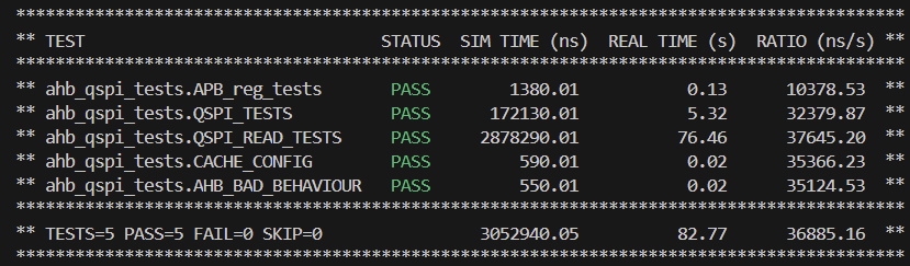
Initial verification of the subsystem. The simulation environment was setup using cocotb, using the AHB extensions to drive the AHB and APB ports of this design. The initial results for the coverage of the tests developed are shown below
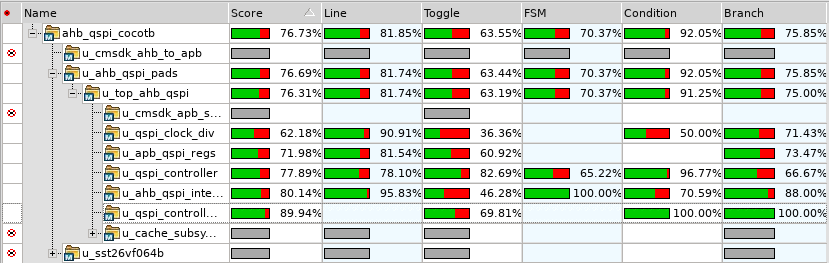
The average coverage from this is 76.73% (ignoring the arm IP coverage and sst26vf064b flash model). After examining the coverage report, some extra tests were added to the cocotb verification. These extra tests covered:
- FSM transitions in u_qspi_controller
- Toggle of bits like address, registers
- Tests to read uncovered branches
These additional tests were executed on a revised version of the sub-system with some tidying up of the implementation, particularly for registers that were too large (such as the clock divider register that was 8 bits, reduced to 5)
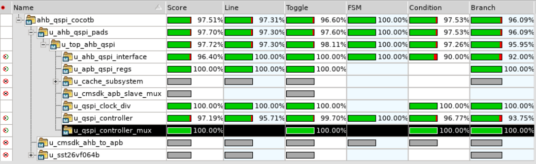
Coverage has so far been improved to 97.51%, with 100% coverage of the FSM in u_qspi_controller. Functionally, the tests are still passing, with assertions to ensure that it is functionally correct.
FPGA Implementation
For the FPGA implementation, a Pynq Z2 board was used with a PMOD SF3. This allowed for simple connection to the QSPI flash. In this case a micron MT25QL256ABA part was used so care had to be taken in order to ensure that the correct commands were sent.
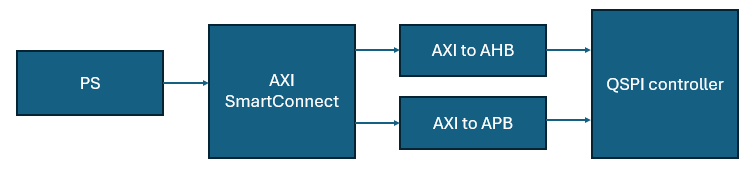
Additional wrappers were added as the PS of the Zynq board is native AXI, so a bridge from AXI to APB and AHB was required as shown below
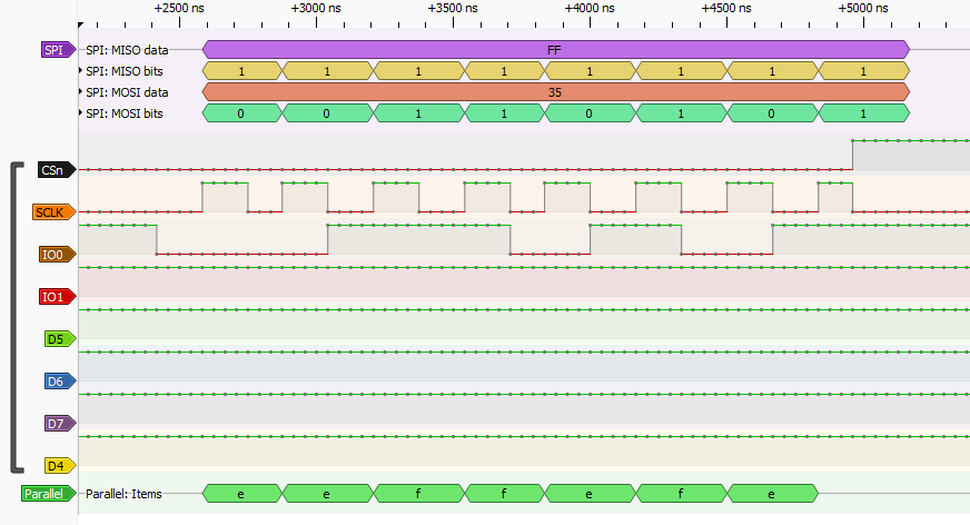
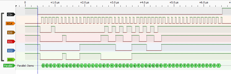
To ensure there was no effect on the timing of the FPGA, an external logic analyzer was used. Some of the verified behaviour is shown below from the logic analyzer. Firstly, a simple opcode transaction (0x35) which sets the QSPI flash in Quad I/O mode.
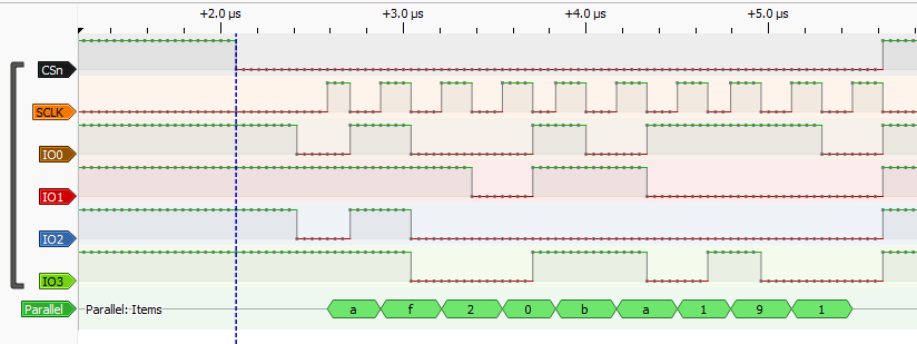
Then a QSPI read ID register transaction (0xAF). This shows that both the OP state and DATA in state are correctly working
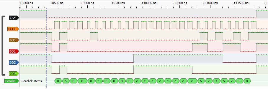
Then a fast read command (0x0B). This was after writing to the flash so here is a test of the OP, ADDR, MODE, DUMMY, DATA I and DATA O states of the qspi controller
And lastly an XiP read over the AHB interface shows that the AHB controller working as expected
SoC Integration
Another verification test was to establish if a SoC design could boot from the QSPI flash. For simplicity, nanosoc is used here. In order to integrate into nanosoc, first the SRAM instruction memory had to be removed and replaced with an instance of the QPSI controller. Secondly the APB subsystem had to be edited to allow for control of the QPSI controller. And lastly top level pads/pins for the QSPI flash were added to the nanoSoC pad ring.

In behavioural verification the code is preloaded on the QSPI, and this works as expected. For the FPGA verification, the code has to be first written to the flash before it can boot.
The first method for programming the flash over FPGA is by using the ADP controller. This is similar to how the existing nanoSoC device is programmed, which is to write directly to the SRAM. However with the QSPI flash, writing has to be enabled, then data written from the controller buffer to the flash (currently only 16 bytes), wait until the flash has finished the write, polling the status register. Using the pynq environment of the Pynq Z2 board, this looks likes below:
file_stats = os.stat('hello.hex')
file_len_in_bytes = round(file_stats.st_size/3)
print(f'file size in bytes is {file_len_in_bytes}')
base_addr=0x0000
addr = base_addr
count = round(file_len_in_bytes/16)
start = time()
with open('hello.hex', mode='r') as file:
for i in range(count):
data = []
for j in range(4):
a=str.strip(file.readline())
b=str.strip(file.readline())
c=str.strip(file.readline())
d=str.strip(file.readline())
tmp = d+c+b+a
data.append((int(tmp,16)))
addr = base_addr + i*16
print(data[0])
QPI_WRITE_ENABLE(adp)
QPI_PAGE_PROGRAM_128(adp, addr, data)
while(QPI_READ_STAT_REG(adp)):
pass
end = time()
length = end - start
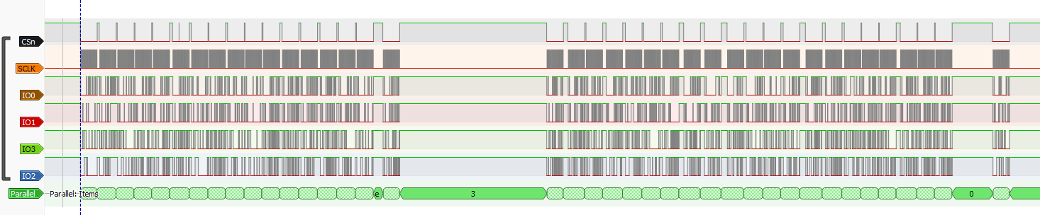
print("Programming took " + str(length), "seconds")It has been verified that the test code runs as expected and the "Hello World" and "Test Passed" messages generated as expected. Below is the QSPI trace for running the hello world program
Physical Design
The plan is to tape out this IP as part of a nanoSoC miniASIC shuttle on TSMC 65nm. Before integrating this into the full nanoSoC design, some constraints for the IP are needed, and some idea on floorplanning.
This design has 3 clocks
- PCLK
- HCLK
- QSPI_SCLK
The QSPI SCLK is generated from the HCLK through a divider. But this is used as the clock internally in the QSPI controller. We must also ensure that the delays of the pins (both inputs and outputs) are clocked to same clock as seen on the output pin of the device.
For TSMC 65nm the constraints can be found here
Floorplanning
As this design uses some memory macros, supplying some recommendations around floorplanning is useful to the implementation engineers. Our initial floorplanning is shown as below
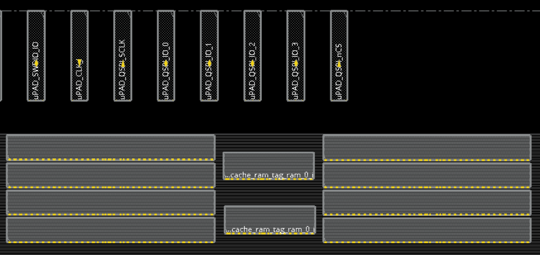
This places the SRAMs for the caches close to the pins (SCLK, IO[3:0] nCS). The 2 smaller SRAMs in the middle are the TAG rams for the caches.
Project Milestones
Do you want to view information on how to complete the work stage ""
or update the work stage for this project?
-
Architectural Design
Design FlowTarget DateCompleted DateHigh level architecture of the AHB QSPI
Result of WorkDone, image for the architecture added to page above
-
Getting Started
Design FlowTarget DateCompleted DateSetup environment for the AHB QSPI IP
Result of WorkEnvironment setup with the Arm IP, simulation environment using the SoCtools git
-
IP Selection
Design FlowTarget DateCompleted DateResult of WorkArm IP used is the CG092 and some of the corstone 101 for the bus infrastructure
-
Behavioural Design
Design FlowTarget DateCompleted DateTake the architectural model and develop the behavioural model
Result of WorkHDL created for the IP
-
Simulation
Design FlowTarget DateCompleted DateSetup the simulation environment and run the initial verification
Result of WorkCompleted simulation with no bugs. Initial verification coverage averages 76.73%
-
Logical verification
Design FlowTarget DateCompleted DateVerify the design, functionally and with coverage
Result of WorkDesign has been verified with coverage of 97.5%
-
RTL Verification
Design FlowTarget DateCompleted DateResult of WorkTested on FPGA with integration in nanoSoC, SoC boots code over the QSPI Flash interface
-
Tape Out
Design FlowTarget DateTarget to tape this out on a TSMC 65nm miniASIC shuttle as part of the nanoSoC chiplet tapeout

Team

 Daniel Newbrook
Digital Design Engineer
at University of Southampton
Research area: IoT Devices
ORCID Profile
 Corstone 101 for m0/m3
 SPI/QSPI
![]() Hardware design
Hardware design
Submitted on
Comments
Tape Out plan
Hi,
Is there a target tape out for this IP?
John.
Tape Out Plan
Hi John
Yes we do have a tape out targeted for this IP. I'm going to add some more detail to the project soon on this subject.
The plan is to tape out nanoSoC with this IP integrated in July 2026 on a miniASIC shuttle. We have already tested and verified the integration of the IP in nanoSoC and shown it to be working on FPGA. I will add some more detail about the backend floorplanning and constraints for this IP to this project
Daniel
New date
Hi,
I see we missed the expected date for this milestone. Perhaps we can put in a new one.
John.
Comparison of Non-Volatile memory
If anyone is interested in the relative merits of the different types of NVM then this article by Tim Daulby might be helpful.
Add new comment
To post a comment on this article, please log in to your account. New users can create an account.