FPGA-Powered Acceleration for NLP Tasks
Project Overview:
Natural Language Processing (NLP) transforms how machines understand and interact with human language. Whether predicting the next word in a sentence, translating languages in real-time, or understanding contextual information from a body of text, NLP applications are increasingly prevalent in various fields such as virtual assistants, translation services, and automated customer support. To meet the growing demand for efficient and real-time NLP processing in embedded systems, we propose designing and implementing a Tiny Transformer Intellectual Property (IP) core. This core will be integrated with an ARM Cortex IP, leveraging the strengths of both the processor system (PS) and programmable logic (PL) parts of a System on Chip (SoC) to create a highly efficient solution for real-time NLP tasks.
Objectives:
1. Design and Implementation of Tiny Transformer IP:
- Develop a compact and efficient transformer IP core using high-level synthesis (HLS), tailored for resource-constrained environments.
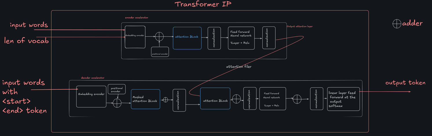
- Include essential components such as an encoder, decoder, attention blocks, normalization layers, and feed-forward neural networks.
2. Integration with ARM Cortex IP:
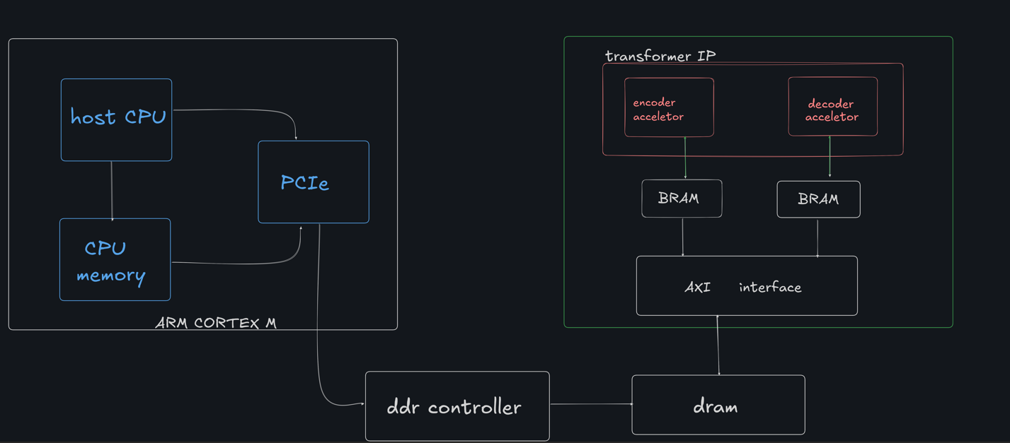
- Utilize the ARM Cortex IP as the processing system (PS) for handling high-level control and preprocessing tasks.
- Integrate the Tiny Transformer IP as the programmable logic (PL) part to accelerate computationally intensive transformer operations.
- Establish seamless communication between the PS and PL using the AXI interface.
3. System Architecture Development:
- Implement a host CPU that interacts with the Tiny Transformer IP via PCIe and manages data flow.
- Integrate BRAM for intermediate storage and a DDR controller for main memory access.
- Optimize the data path and memory hierarchy to ensure low-latency and high-throughput processing.
4. Performance Evaluation:
- Benchmark the integrated system against conventional CPU-only implementations to demonstrate improved performance.
- Assess power consumption and resource utilization to validate the efficiency of the Tiny Transformer IP in embedded scenarios.
Expected Outcomes:
The successful completion of this project will result in a highly optimized Tiny Transformer IP core integrated with an ARM Cortex IP. The project will generate a complete RTL to GDSII flow, enabling the tape-out of our accelerator on a 65nm technology node. This integration will provide a robust solution for deploying transformer-based models in resource-constrained devices, enabling real-time processing of NLP tasks with significantly reduced latency and power consumption. This advancement will pave the way for sophisticated applications in IoT devices, edge computing, and mobile platforms, making advanced NLP capabilities more accessible and efficient.
Project Milestones
Do you want to view information on how to complete the work stage ""
or update the work stage for this project?
-
Architectural Design
Design FlowTarget DateCompleted DateProject Kickoff:
- Define project objectives and scope.
- Review existing technologies and research relevant to Tiny Transformers and ARM Cortex integration.
-
Behavioural Design
Design FlowTarget DateCompleted DateDesign Phase:
- Develop initial architecture for Tiny Transformer IP.
Begin high-level synthesis (HLS) of essential transformer components (encoder, decoder, attention blocks).
-
Behavioural Design
Design FlowTarget DateCompleted DateImplementation Phase:
- Complete HLS of Tiny Transformer block components of input embedding.
- Develop communication protocols between PS and PL parts of the SoC.
-
Behavioural Design
Design FlowTarget DateCompleted DateSystem Architecture Development:
- Implement attention block and normalization block.
-
Accelerator Design Flow
Design FlowTarget DateCompleted Dateimplemented encoder block with hardware utilization as 22 % LUTS and 7 % BRAM.
-
Milestone #6
Target Date -
Milestone #7
Target Date -
Milestone #8
Target Date -
Milestone #9
Target Date -
Milestone #10
Target Date -
Milestone #11
Target Date -
Milestone #12
Target Date -
Milestone #13
Target Date
Team
 Project Creator
at Indian Institute of Technology Jodhpur
![]() Accelerators
Accelerators
![]() Hardware design
Hardware design
![]() Accelerator Design Flow
Accelerator Design Flow
Submitted on
Comments
Tiny-Trans
Team Members:
Abhishek Yadav (yadav.49@iitj.ac.in)
Ayush Dixit (m23eev006@iitj.ac.in)
Binod Kumar (binod@iitj.ac.in)
Add new comment
To post a comment on this article, please log in to your account. New users can create an account.