Aspen: A 630 FPS Real-Time Posit-Based Unified Accelerator for Extended Reality Perception Workloads
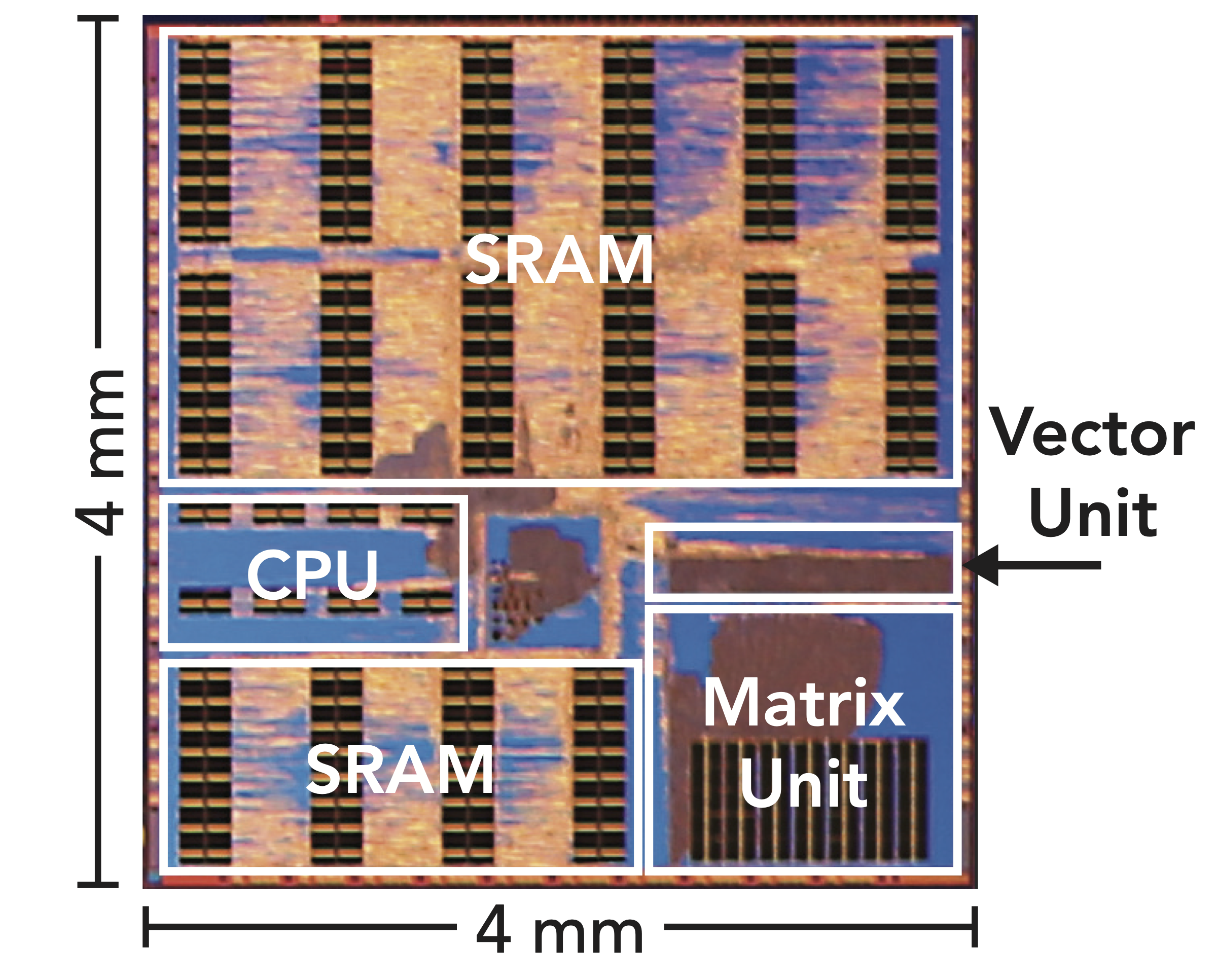
Aspen is a unified accelerator for deep neural network (DNN)-based extended reality perception workloads. Aspen proposes a mixed-precision quantization scheme using the posit datatype to reduce memory usage while maintaining accuracy, a DNN accelerator for mixed-precision posit datatypes, and efficient data prefetching and data layout to minimize data reorganization. The Aspen system-on-chip has an Arm Cortex-M3 CPU, a mixed-precision posit-based DNN accelerator, and 4 megabytes of SRAM partitioned into eight 512 KB banks, connected through a 128-bit-wide interconnect. The DNN accelerator consists of a matrix unit and a vector unit. Aspen is fabricated in Intel 16 and achieves real-time processing of visual inertial odometry, eye gaze extraction, and object classification at 98.9, 630, and 31 frames per second, respectively.
Project Milestones
Do you want to view information on how to complete the work stage ""
or update the work stage for this project?
-
Getting Started
Design FlowTarget DateCompleted Date -
Getting Started
Design FlowTarget DateCompleted Date -
Getting Started
Design FlowTarget DateCompleted Date -
Getting Started
Design FlowTarget DateCompleted Date -
Getting Started
Design FlowTarget DateCompleted Date -
Getting Started
Design FlowTarget DateCompleted Date -
Getting Started
Design FlowTarget DateCompleted Date -
Getting Started
Design FlowTarget DateCompleted Date -
Getting Started
Design FlowTarget DateCompleted Date -
Getting Started
Design FlowTarget DateCompleted Date -
Getting Started
Design FlowTarget DateCompleted Date -
Getting Started
Design FlowTarget DateCompleted Date -
Getting Started
Design FlowTarget DateCompleted Date -
Specifying a SoC
Design FlowCompleted Date -
data model
Design FlowCompleted Date -
IP Selection
Design FlowCompleted Date -
Universal Verification Methodology
Design FlowCompleted Date -
Behavioural Modelling
Design FlowCompleted Date -
Behavioural Design
Design FlowCompleted Date -
Generate RTL
Design FlowCompleted Date -
RTL Verification
Design FlowCompleted Date -
Simulation
Design FlowCompleted Date -
Logical Design
Design FlowCompleted Date -
Technology Selection
Design FlowCompleted Date -
Synthesis
Design FlowCompleted Date -
Design for Test
Design FlowCompleted Date -
Logical verification
Design FlowCompleted Date -
Physical Design
Design FlowCompleted Date -
Floor Planning
Design FlowCompleted Date -
Clock Tree Synthesis
Design FlowCompleted Date -
Routing
Design FlowCompleted Date -
Timing closure
Design FlowCompleted Date -
Physical Verification
Design FlowCompleted Date -
Tape Out
Design FlowCompleted Date -
Post Silicon
Design FlowCompleted Date

Team
 Project Creator
Research Assistant
at Stanford University
Research area: Electrical Engineering
 Cortex-M3
 Socrates Interconnect tool
Submitted on
Comments
Aspen: Accelerator for Extended Reality Perception
Hi,
Thank you for submitting this project it looks very interesting. I noticed in your IEEE paper that the M3 had 32Kb Data and Instruction caches. There were also two DMA engines? and 4 additional 32 Kb SRAM blocks. There was no description of these in the paper. Which DMA engines did you use, were these Arm IP?
We use both the DMA PL230 and DMA 350 Arm IP in the nanoSoC reference design.
We look forward to hearing from you.
John.
Add new comment
To post a comment on this article, please log in to your account. New users can create an account.