






megaSoC Prototyping using HAPS-SX
This design flow stage enables the deployment, evaluation and pre-silicon ASIC prototyping of large SoC designs using a Synopsys HAPS-SX, a modular, high-capacity and high-performance FPGA-based system. At SoC Labs, a HAPS-SX system with an AMD-Xilinx Virtex UltraScale+ VU19P FPGA, which has 8,938K logic cells, and a total of 90 Mb BRAM, is used to prototype the megaSoC design by mapping the RTL onto FPGA hardware for system-level validation.
Connecting to the HAPS system
The HAPS-SX system is managed as a virtual service by a dedicated control host (computer), which provides system management, FPGA programming, and runtime access to the HAPS-SX chassis. The HAPS-SX system typically connects to the control host via a high-bandwidth UMRBus (Universal Multi-Resource Bus) over a PCIe interface, using the provided MGB (Multi-Gigabit Board) adapter kit, or via Ethernet. The PCI Express connection is used for high-speed FPGA programming and runtime communication between the control host and the design running on HAPS-SX, while the Ethernet connection is used for design I/O, software-driven validation, or network-based communication. These connections provide access to interfaces such as JTAG and UART and support system configuration, reset control, and console output monitoring, allowing developers to interact with, and debug, the running SoC prototype.
Users do not connect directly to the HAPS-SX chassis. All user interaction occurs through the control host using remote access protocols such as Secure Shell (SSH). The control host must run a Synopsys-supported Linux distribution. Supported operating systems are listed in the HAPS Installation and Release Documentation.
At SoC Labs, the FPGA is accessed remotely for programming and debugging through the Xilinx Virtual Cable (XVC) protocol, allowing Vivado's Hardware Manager to connect to the HAPS-mounted VU19P over the network as though it were a locally attached JTAG target.
Configuring the HAPS system
Comprehensive instructions for setting up the HAPS system are provided in the HAPS Installation and Release Documentation.
Synopsys provides dedicated HAPS configuration tools for system configuration. Most HAPS environments include:
- HAPS ProtoCompiler / ProtoCompiler DX - partitioning, synthesis orchestration, build flow, database, etc.
- HAPS system configuration - power, clocks, connector power, resets, programming mode, etc.
- Debug/visibility tools - often Identify / HAPS debug environment, depending on your licenses, etc.
FPGA vendor tools are used for the programming of the FPGA devices. Similarly to nanosoc, at SoC labs, Xilinx's Vivado Design Suite is used. Xilinx's Vivado software suite provides a comprehensive toolset for developing FPGA designs. It is essentially a tool that turns an RTL design into a bitstream that runs on the FPGA.
Board configuration via ConfPro
Before any design will run on the HAPS-SX, the board's I/O bank power and clock generators must be enabled through the ConfPro (HAPS-SX Configuration) tool. This is an external board-setup step that is invisible to Vivado, and it is a required precondition for every hardware run.
Two settings are critical for the megaSoC prototype:
- System clock frequency. The clock feeding the design (GCLK1) must be set to match the design's timing constraints. This is done in the ConfPro Clock tab, followed by Configure System.
- I/O bank power. Any bank carrying user I/O must be powered at the correct voltage. For the current megaSoC pin set, the clock, reset, LED, PMOD and SPI-flash pins all reside on fixed-1.8V banks (20, 21, 83), so no JX power configuration is required; designs that use HapsTrak connectors must enable the relevant JXn_VCCO rails.
Without this configuration, the input clock never reaches the FPGA, and the design appears completely dead: the heartbeat LED does not toggle, the CPU does not boot, and Vivado's debug hub (and therefore any ILA) cannot be detected after programming.
Overall Prototyping Flow
The prototyping process follows these stages:
RTL integration
Simulation-based validation
FPGA synthesis and implementation
Bitstream generation
Deployment to HAPS hardware
Hardware debug and validation
1. RTL Integration
The MegaSoC reference design is an Arm Cortex-A53-based SoC designed for research projects and targeting an ASIC tape-out. The original A53 compute system RTL within the Arm AAA IP bundle targets an ASIC flow. The work described here adapts the RTL for pre-silicon validation on an FPGA. This supports an FPGA verification environment that can speed up the full SoC design process, which may include any research-specific IP.
| Task | Status | |
I | HAPS board configuration (ConfPro) | Complete |
II | FPGA top-level wrapper | Complete |
III | ASIC SRAM macro replacement models | Complete |
IV | Clock gate cell stub | Superseded — gating now bypassed |
V | XDC pin constraints | Complete |
VI | UART0 routing | Complete |
VII | DRAM AXI error slave | Complete |
VIII | Reset restructuring (async-assert / sync-deassert) | Complete |
IX | QSPI controller reclocking | Complete |
X | Timing closure (hold) | Ongoing |
XI | DDR4 controller integration | Ongoing |
I. HAPS board Configuration. As described above, the board's clocks and I/O bank power are configured through ConfPro before each hardware run. This step is part of the bring-up and is documented here because a missing or incorrect ConfPro configuration is the most common cause of an apparently dead design.
II. FPGA top-level Wrapper. The megaSoC RTL is integrated into a top-level wrapper (haps_top), which adapts the SoC design to the FPGA environment (as opposed to the ASIC flow).
The key contributions of this wrapper are:
- clock input handling
- reset synchronisation and delayed release
- generation of an internal real-time clock
- heartbeat signal generation
- UART signal routing
- QSPI interface breakout
III. ASIC SRAM macro replacement models. The ARM Cortex-A53 RTL instantiates foundry SRAM macros that are not available in the FPGA flow. A simulation shim library provides behavioural replacements for all of the necessary macros, matching each macro's port list and read latency. This allows the Arm-delivered wrapper RTL to be left unmodified, while a separate simulation model file provides FPGA-compatible definitions. These models are for FPGA bring-up only; the real compiled macros return for the ASIC flow, where their actual timing must be verified in the later gate-level simulation design flow stage.
NOTE: The shim must match each macro's read latency behaviour, not merely its latency figure. The two-cycle model used for the L2 data banks originally gated its output pipeline stage on the current cycle's chip-enable, so any read not immediately followed by another access never reached the output register and returned stale data. Sixteen instances sit in the CPU's instruction and data return path. The output stage must be advanced by a one-cycle-delayed enable, as a real macro does.
IV. Clock gate cell stub. On ASICs, clock gating is safe: clock trees are balanced as part of physical design. FPGAs implement clock networks with dedicated global buffers, and gating them in fabric degrades the clock — a behavioural integrated clock-gate model synthesises to a latch (LDCE) plus a LUT on general routing, with skew that is uncontrolled relative to the global net.
An earlier version of this flow supplied a stub modelling the gate as a latch-based gated clock so the design would elaborate and synthesise. That stub is retained only for the ASIC flow. On FPGA, clock gating is now bypassed entirely: every gate cell passes the clock through unmodified, placing the whole SoC on a single global buffer with one clock latency. Gating is a power-saving feature with no functional meaning on a prototype.
This applies to all four gate cells in the design — the Cortex-A53's cells, PCK600 (which clocks the power controllers sequencing CPU reset release), GIC400, and the CTI gate.
V. XDC pin constraints. An XDC constraints file maps the top-level ports to the HAPS-SX VU19P package pins. Pin assignments were verified against the HAPS-SX VU19P 1F System Reference Manual. Note that the system clock is an LVDS differential pair (GCLK1) and must be brought in through an IBUFDS primitive; it is not a single-ended input. UART is routed to the PMOD3 connector, which is physically accessible. The pin assignments are listed below:
| Signal | Package Pin | Function |
| HAPS_CLK_IN | BM44 / BN44 | System clock - GCLK1 |
| HAPS_RESET_N | BK44 | Active-low reset - PB1 (push Button) |
| HB | BF14 | Heartbeat LED - LED5 |
| UART_TX | BE18 | UART transmit - PMOD3 IO[0] |
| UART_RX | BE19 | UART recieve - PMOD3 IO[1] |
| PL011_tx | BG19 | Secondary UART transmit - PMOD3 IO[2] |
| QSPI_SCLK | CA49 | Flash serial clock |
| QSPI_nCS | CB49 | Flash chip select |
| QSPI_IO[0] | CC49 | Flash data 0 |
| QSPI_IO[1] | CC50 | Flash data 1 |
| QSPI_IO[2] | CA51 | Flash data 2 |
| QSPI_IO[3] | CB51 | Flash data 3 |
Banks 20, 21 and 83 are fixed at 1.8V, so no JX connector power configuration is required for this pin set.
VI. UART0 routing. A direct UART0 bypass exposes the UART0 transmit and receive signals before the GPIO pin mux (under an ifdef FPGA_BUILD guard). This was necessary because the bootrom prints over UART0 but configures the GPIO pin-mux FUNC register only later in boot, after the SRAM test — meaning early output would otherwise be invisible. The bypass makes the boot output observable during bring-up. It also exposed a latent firmware ordering issue (the bootrom should configure the pin mux before transmitting), which must be addressed for silicon, where there is no bypass. The bypass itself is FPGA-only and is removed for the ASIC flow.
VII. DRAM AXI error slave. The NIC400 DRAM port has no responder until the DDR controller is integrated. An AXI4 error slave terminates this port, returning a DECERR response for all transactions and correctly handling AXI burst protocol. This prevents the CPU from hanging indefinitely if the MMU page tables map DRAM addresses and a speculative access reaches the unconnected port. It is a placeholder to be replaced by the real DDR controller.
FPGA block design for SoC test-bench
An FPGA block design defines how the SoC RTL and supporting infrastructure are integrated within the HAPS-SX environment.
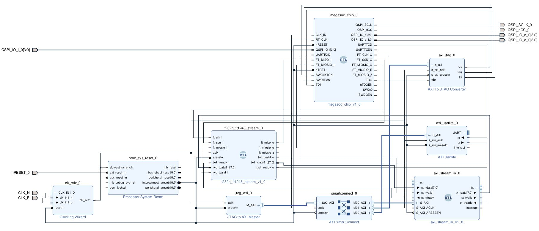
The above image shows the block diagram for the FPGA debug environment. This includes a JTAG to AXI component, which uses the Xilinx Virtual Cable to interface with the JTAG side. tcl commands are used to write to that AXI interface (as seen here). This AXI interface then drives: a UART component, a JTAG component, and an FT1248 component. The UART is connected to the UART peripheral within MegaSoC, and the JTAG is connected to the DAP-lite that is used to debug the Cortex A53. The FT1248 component connects to the ADP controller in megaSoC.
The ADP controller was originally created as an easy-to-use debugger for the nanoSoC. It takes an ASCII character as input and generates AHB-lite commands to the SoC. The addition of the ADP controller in megaSoC may only be temporary as we assess its suitability for this full AXI system. But this does, however, enable the reuse of SoC Labs resources and a known use case for debugging in an FPGA.
By instantiating these interfaces alongside the SoC logic, the prototype supports real-time validation of the megaSoC behaviour and provides mechanisms to use standard debug tools.
For initial bring-up, a lighter-weight path was also used: an Integrated Logic Analyser (ILA) instantiated directly in the top-level RTL, observing the heartbeat counter, reset state, UART transmit line, and QSPI chip-select. This allows the core health of the design (clock alive, reset released, CPU booting, UART active) to be confirmed over XVC without additional physical wiring.
2. Simulation-Based Validation
Before FPGA synthesis, the system is validated in simulation. The checks performed are:
- reset release
- internal counter activity
- heartbeat toggling
- CPU AXI transactions (fetch/read/write)
- peripheral bus activity
- UART output observation
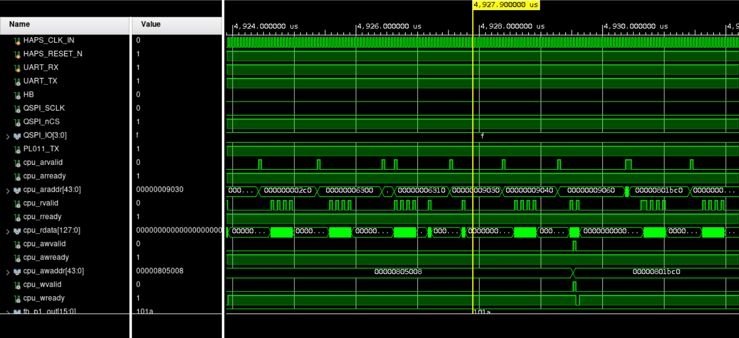
Simulation confirms the expected boot progression: the CPU comes out of reset, fetches from the bootrom, enters the main boot code, begins the SRAM memory test, and configures the GPIO peripheral. One practical finding is that the SRAM memory test dominates simulation time: the MMU maps the SRAM region with device-type (non-gathering, non-reordering, no-early-write-acknowledge) memory attributes, which serialises every AXI transaction. As a result, simulating all the way to the boot banner is impractical, and the banner is most usefully observed on real hardware, where the same boot completes in well under a second.
3. FPGA Synthesis and Implementation
The design is synthesised and implemented in Vivado targeting the VU19P (xcvu19p-fsva3824). The FPGA_BUILD define is supplied at synthesis time so that the FPGA clock-path and UART bypass adaptations are selected, while simulation builds omit the define and use the behavioural clock controller. Timing closure is achieved at 20 MHz; the differential clock is brought onto the global clock network through an IBUFDS and BUFG.
4. Bitstream Generation and FPGA Programming
A single build script drives synthesis, optional ILA insertion, implementation, and bitstream generation. The resulting bitstream and its probes file are programmed onto the HAPS-mounted VU19P over XVC using Vivado's Hardware Manager (connecting to the board's XVC URL). The ConfPro clock and I/O configuration described above must be applied before, or immediately after, programming for the design to run.
5. SoC Emulation and Validation
Once programmed and clocked, the design's health is confirmed on hardware. The heartbeat LED (and the ILA heartbeat probe) confirms the clock path and reset release; activity on the UART transmit line after reset confirms that the CPU has booted and the bootrom firmware is running. A 1.8V-compatible USB-UART bridge connected to the PMOD3 connector provides a serial console at 115200 baud for reading boot output directly.





Add new comment
To post a comment on this article, please log in to your account. New users can create an account.