nanoSoC Low Power Implementation
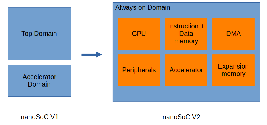
As part of plans for continued development of nanoSoC one area that requires improvement is the power structure of system. The first iteration of nanoSoC contained 2 power domains: the accelerator domain and the remainder of the SoC. Both power domains were connected to external pins to allow connection to separate external voltage regulators and power measurement ICs, as implemented in the first version of the nanoSoC testboard. This allowed for measurement of the power/energy usage of the custom accelerator but did not allow for fine grained measurement of key parts of the SoC infrastructure. Publishing energy figures for hardware accelerators is important for demonstrating research outcomes. However, the accelerator itself doesn't exist in a vacuum, and understanding more about the energy used for tasks such as data movement, pre/post-processing data in CPU, and external communication can help guide the academic community to better low-power designs.
For these reasons, this project is looking to incorporate better power structure and control into the nanoSoC reference design as part of a version 2 of the design. This task can be broken down into the following sub-tasks
- Power structure:
- Define which domains to focus on separate of concerns within the design
- Introduce these power domains into the backend ASIC flow
- Power control:
- Define which blocks can be turned off/on
- How to control these blocks power state
- Implement power control in the behavioural RTL
- Clock control:
- Define where clock gating can occur
- Implement clock gating in the behavioural RTL
- Power monitoring
- Define which blocks need monitoring
- Describe how these blocks will be monitored
- Implement internal/external power monitoring
Power Structure
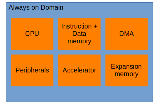
One initial view of how to separate the power hierarchy would be to follow roughly the system design hierarchy taking into account the main SoC architecture, i.e. CPU, IMEM+DMEM, DMA, peripherals, accelerator and expansion memories. The exact partition between some of these blocks and the always-on domain will be slightly blurred, as some parts of each block will have to remain "always-on" so that they can wake up the parts of the subsystem that have been put into a low power mode. This gives a good first idea of where to draw the partitions.
CPU
The Cortex M0 integration kit actually comes with an example power intent and internal power controller. This power control can put the "debug" and "sys" components to a low power mode when the CPU is in a sleep mode.
- SoCLabs M0 wrapper
- prmu (power controller)
- Cortex M0 Integration layer
- Cortex M0
- SYS (can be put to sleep)
- DBG (can be put to sleep)
- Cortex M0 DAP
- AP (can be put to sleep)
- Cortex M0 WIC
- Cortex M0
For this project the power intent scripts as supplied from Arm will be used (for simplicity). These include 3 power domains: Top, debug and sys. The Top domain will be a part of the always on domain.
On-chip Power Network
To obtain fine grain measurement and control over the power domains, some on chip power distribution and monitoring has to be incorporated. For a simple power monitoring solution the same supply network as the original nanoSoC can be used, adding monitoring points for each of the power domains.
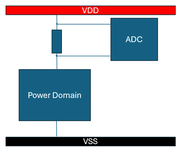
The sense resistor in this case could be from the power switches that will be used for the switched power domains. This could be extended further to have on chip voltage scaling, by using some controllable voltage regulators. For this project the monitoring is the main focus.
In order to successfully implement this structure the actions needed are:
- Back end flow changes to include the introduction of power switches
- ADC
- Analog mux
- Differential amplifier with programmable gain
Programmable gain of the differential amplifier will be used to increase/decrease the sensitivity of the current measurements. It may not be known until implementation what the current draw from each of the domains is, or if the power switches are used as sense resistors, what resistance they will actually give.
Project Milestones
Do you want to view information on how to complete the work stage ""
or update the work stage for this project?
-
Getting Started
Design FlowTarget DateCompleted DateCreate a general plan for the project to take place
-
IP Selection
Design FlowTarget DateCompleted DateMost IP for this project will be custom made, but Arm IP may include the PCK-600
-
Architectural Design
Design FlowTarget DateOverall architectural design of the power structure and power control for nanoSoC. This may include adding the PCK IP from Arm
-
Behavioural Design
Design FlowTarget DateDesign of the analog subsystem and components including, OPAMP, ADC, analog MUX.
-
Behavioural Modelling
Design FlowTarget DateModelling of the subsystem IP and integration with the sense resistor (possibly a switch from the Arm standard cell libraries)
-
Technology Selection
Design FlowTarget DateCompleted DateFirst this project will be carried out for TSMC 65nm (as this is what nanosoc V1 was taped out using)
Result of WorkTSMC 65nm chosen
Team


 Daniel Newbrook
Digital Design Engineer
at University of Southampton
Research area: IoT Devices
ORCID Profile
 Cortex-M0
 CoreLink DMA-230
 PCK-600 Power Control Kit
![]() Low power design
Low power design
![]() Physical Design
Physical Design
Submitted on
Add new comment
To post a comment on this article, please log in to your account. New users can create an account.