




megasoc re-usable SoC platform
Rationale
megasoc has been designed to provide a complex SoC component that can 'host' and support the development and evaluation of research components or subsystems. The design allows for seamless transition from FPGA to physical silicon implementation via a pre-verified programmable control system that allows reuse of software and diagnostic functionality to facilitate the configuration, control and diagnostic analysis of research hardware such as custom accelerators or signal processing.
The design is based on an Arm Cortex-A53 CPU core with inspiration from the Corestone 1000 subsystem from Arm. megasoc allows the reuse of the AAA pre-verified IP, documentation and software but it is architected to support simple 'bolting-on' of experimental hardware. The aim of megasoc is to provide a fully Linux capable SoC whilst minimising the cost of physical silicon production.
Technical Overview
megasoc is a complex SoC utilising the Cortex-A53 processor with pad-level support for silicon implementation. Included is:
- CPU - Armv8-a Cortex A53 processor
- Interrupt Controller - GIC 400
- Software Debugger - Arm DAP-lite
- Boot ROM
- XiP QSPI - For program or BIOS
- SRAM
- NIC 400 System Bus
- DRAM controller
- DMA for system support - Off-chip mem to DRAM
- Peripherals (UART, Timers, etc)
Ideally we plan to integrate some high speed off-chip interfaces, but currently we are making a 'Minimal Viable Product' using the IP that has already been obtained. In the future we would like to integrate:
- PCIe
- Gigabit Ethernet
- USB
For the current implementation please refer to "megaSoC V1 - Architectural Changes" below.
Architecture
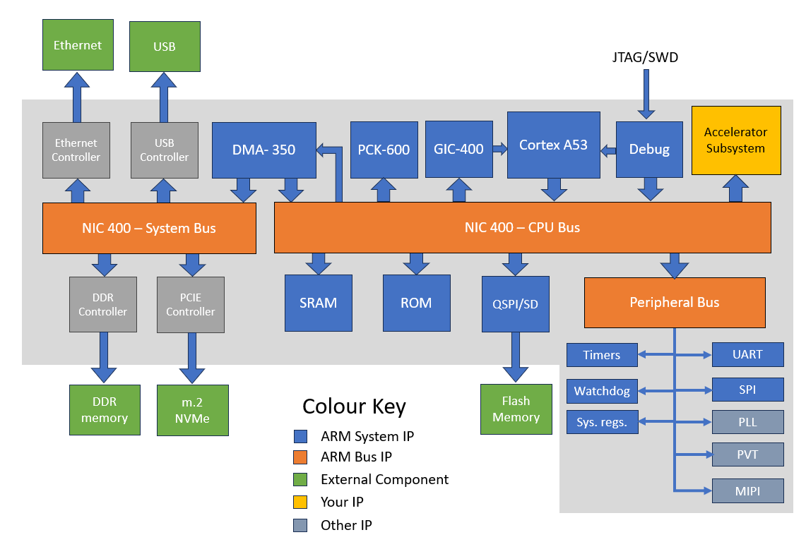
The overall architecture is as shown below. This has been separated into 2 main sections, the CPU and System sections. Development so far has been focused on the CPU subsystem (with the DDR controller implemented on the CPU bus). We are currently exploring options for sourcing the IP for the ethernet, USB and PCIe controllers.
Address Map
The Cortex A53 has a 40-bit address interface, this gives a total addressable space of 1 TB. For now a simplified 33 bit address map is being created, it is likely that any higher address will be used to expand the DRAM and possibly for direct access from the CPU to the communication interfaces (PCIe, USB, Ethernet) if possible, although these will all likely be controlled by DMA transfers.
Currently this address map is unoptimised (some regions are much larger than necessary, and there are a few empty regions which will likely be filled as development progresses.
| Start Address | End Address | Region | Size |
|---|---|---|---|
| 0x000000000 | 0x00000FFFF | Boot Rom | 64 KiB |
| 0x000400000 | 0x0007FFFFF | QSPI Flash | 4 MB |
| 0x000800000 | 0x00087FFFF | SRAM | 512 KiB |
| 0x001000000 | 0x00100FFFF | Flash and Cache Control | 64 KiB |
| 0x001010000 | 0x00101FFFF | SDIO Control | 64 KiB |
| 0x001100000 | 0x001107FFF | GIC 400 | 32 KiB |
| 0x001200000 | 0x001207FFF | Power Control (PCK600) | 32 KiB |
| 0x001300000 | 0x001307FFF | Debug | 32 KiB |
| 0x001500000 | 0x001506FFF | DRAM Controller Config | 28 KiB |
| 0x002000000 | 0x0027FFFFF | DRAM PHY Config | 8 MiB |
| 0x040000000 | 0x05FFFFFFF | Peripheral | 512 MiB |
| 0x060000000 | 0x060FFFFFF | Expansion manager | 16 MiB |
| 0x080000000 | 0x27FFFFFFF | DRAM | 8 GB |
CPU Interrupts
The GIC-400 generic interrupt controller supports a maximum of 480 shared interrupts. Currently implemented interrupts sources are shown below, higher interrupts are tied off to 0's
| IRQ Number | Source |
|---|---|
| 32 | DMA350 Channel 0 interrupt |
| 33 | DMA350 Channel 1 interrupt |
| 34 | DMA350 Channel 2 interrupt |
| 35 | DMA350 Channel 3 interrupt |
| 36 | DMA350 common interrupt |
| 37 | GPIO Port 0 combined interrupt |
| 38 | GPIO Port 1 combined interrupt |
| 39 - 54 | GPIO Port 0 Pin 0-15 interrupts |
| 55 - 70 | GPIO Port 1 Pin 0-15 interrupts |
| 71 | Timer 0 Interrupt |
| 72 | Timer 1 Interrupt |
| 73 - 75 | Dual timer interrupts |
| 76 - 80 | Synchronous UART 0 Interrupts |
| 81 - 85 | Synchronous UART 1 Interrupts |
| 86 - 90 | UART 0 Interrupts |
| 91 - 95 | UART 1 Interrupts |
| 96 | Watchdog interrupt |
| 97 | RTC Interrupt |
| 98 - 102 | SPI Interrupts |
| 103 - 108 | PL011 (RS232 UART) Interrupts |
| 109 | QSPI Interrupt |
| 110 - 117 | Expansion region interrupts |
| 118 | SDIO Interrupt |
| 119 - 126 | DRAM Interrupts |
| 127 - 130 | Ethernet Interrupts |
Communication channel
Currently implemented are 4 UART channels. USRT 0 & 1 are connected to the HOSTIO Debug controller, these channels can be used for debug purposes and STDIO. They will require an off-chip HOSTIO controller (currently work on implementing this in a raspberry PI RP2040 chip)
The other 2 UARTs are for general communication and can easily be used with a number of debug connections. Currently the thought will be to use a FT232 chip on the PCB to act as a USB - UART and allow for very simple debug information.
As described in "megaSoC V1 - Architectural Changes" we have also added a PL011 UART interface. The purpose for this is to act as a fully handshaked UART (CTS, DSR, DCD, RTS, DTR signalling included) which can be used for networking over serial.
Pinlist
| Pin/Port | Function |
|---|---|
| REF_CLK_XTAL1/2 | Main System clock from crystal oscillator |
| RT_CLK_XTAL1/2 | Real time clock input from crystal oscillator |
| PORESTn | Active low power-on-reset |
| nSRST | Active low System reset |
| SWD/JTAG | Mictor 38 interface for Arm debug |
| GPIO_P0[15:0] | GPIO Port 0 |
| GPIO_P1[15:0] | GPIO Port 1 |
| QSPI_SCLK | Clock output from QSPI controller |
| QSPI_nCS | Chip select output from QSPI controller |
| QSPI_IO | Data I/O from QSPI controller |
| PL011 Interface | Full UART interface with handshaking signals |
| DRAM interface | |
| SDIO Interface |
Using megaSoC
If you'd like to use megasoc for your custom hardware, you can fork or clone the megasoc project git repository. This SoC reference design is still under development, expand the V1 Tapeout section below for more details.
megaSoC V1 Tapeout
- megaSoC V1 - Architectural Changes
Work is currently underway to tapeout megaSoC in 2026. This initial version will be a "Minimal Viable Product" version of megaSoC. This version will not have the complexity of high speed external interfaces and the PCIe, USB and Ethernet subsystems.
The aim for the initial tapeout of megaSoC is to prove the core compute system, the fabrication flows and provide a good baseline of information to the community on taping out an A-class processor on an advanced technology node. As with the first version of nanoSoC some application scenarios may be limited it will serve as a good foundation for future improvements.
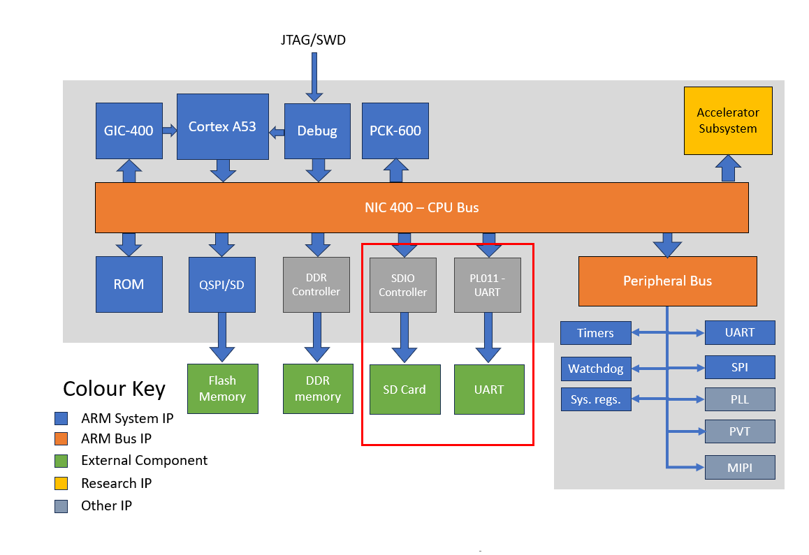
These two controllers will be replaced with an SDIO controller (ZipCPU SDIO) and a UART controller (PL011 from ARM)
Network
Whilst not ideal, networking is possible over UART. The initial plan for the MVP implementation of this megaSoC-lite version was to use this approach. Network communication is possible using packages like PPP in linux (an example on how to set this up between 2 raspberry pi's). The PL011 from Arm has been chosen as it allows for hardware flow control which is ideal for this application.
We are also looking into using an Ethernet mac subsystem with an RMII interface that would allow for 100 Mbps networking (much faster than over UART). Work is currently being done on integrating this into nanoSoC here. The Ethernet MAC controller and PTP timer have now been instantiated in megaSoC but are not yet verified.
SD card filesystem
Ideally a very high speed non-volatile memory would be used for the filesystem using a PCIe interface to integrate an M.2 SSD device. However, it is quite common practice to use SD cards for such applications. The implementation of a PCIe interface and associated PHY for the SD controller is a target for a later version. The ZipCPU project is mostly focused around FPGA implementations. Whilst there is a lot of information available it would require a custom PHY implementation. Without a PHY the system would be limited in the bandwidth achievable for the SD card.
DDR Controller + PHY
For this project, Synopsys have kindly donated their DDR controller and PHY IP to SoClabs. The specific parts used in this project are the uMCTL2 DDR controller and LPDDR4 multiPHY. This will allow for an implementation of megaSoC as a single board computer (SBC), with LPDDR4 module on the PCB. For this initial prototype of the project we are keeping this as simple as possible using a 16 channel LPDDR4 device (most likely something like the D1611PM3BDGVIW-U device from Kingston technology).
For this configuration we are using a 16 Gbit (2GB) device, which we believe will give us a good starting point to ensure enough memory for the OS performance, whilst keeping complexity and cost to a minimum.
- Verification
Behavioural Verification
- Backend - Hierarchical design Planning
As the megaSoC design is a large SoC, the backend work must be done using a hierarchical/bottom up approach. This means dividing the design into sub-blocks, performing backend on each of those blocks and then bringing the whole design together.
Synopsys Fusion compiler includes a flow for hierarchical design planning that also allows you to break the design into blocks but run the backend in parallel for each of those sub-blocks. This ensures all blocks are in sync at each of the design steps and you can run verification after each point (e.g. post clock opt gate simulations/logical equivalence)
Floorplan
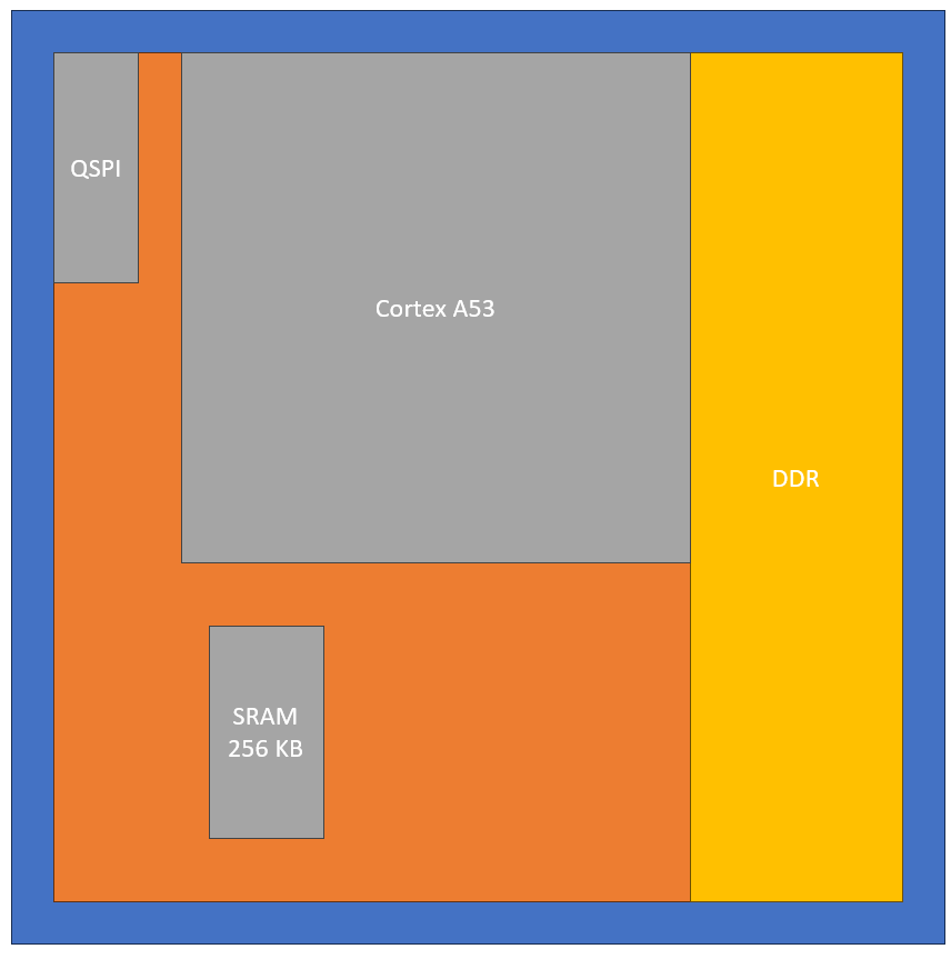
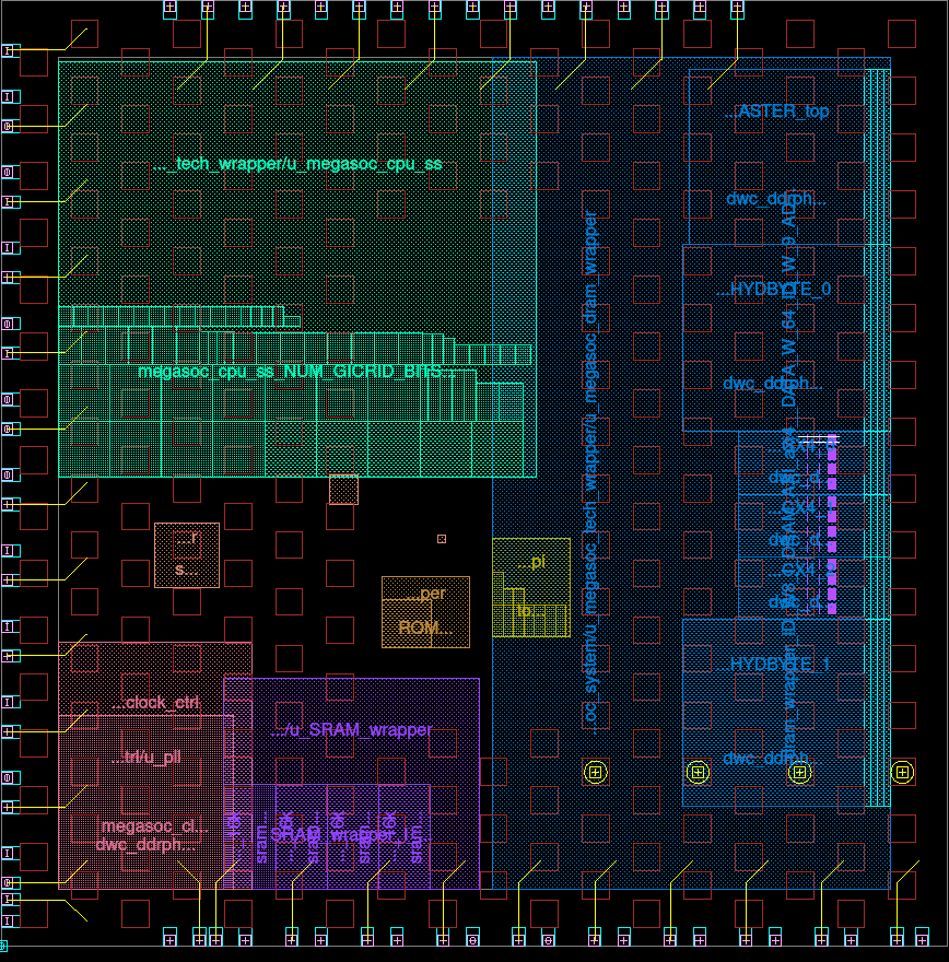
It is a good idea to have an initial floorplan of how the blocks will be split up. Below is our initial estimate for what the floorplan will look like. We expect the A53, DDR, SRAM and QSPI controllers to be the largest IPs that should be worked on hierarchicaly. The NIC400 bus to also expected to be fairly large, but may be best for this to be merged into the top hierarchy as it will likely be distributed across the entire chip.
In terms of IO; we are expecting that the die will be about 2.2 x 2.2 mm, using a bump pitch of 200um we can have a total of 121 IOs (linearly arranged). The number of IOs to be supported by the SoC funcitonality is as follows:
- Clocks + resets - 3
- SWD/JTAG - 6
- QSPI - 6
- GPIO - 32
- UART (RS232) - 10
- LPDDR4 - 39
- SDIO - 7
This gives a total of 103 for the signal pins. Leaving 18 bumps for power and ground, ~ 4 per side (VDD, VSS, VSSIO, VDDIO).
Using the equations from the datasheet given with the GPIO libraries, we can calculate based on the number of GPIO's used, that would need 16 VDDIO/VSSIO cells. We need to revisit the total number of bumps to accomodate the power supply pins needed.
For now we are going to assume that the die size stays the same, but we will reduce the bump pitch to 150 um. This would give us a total of 196 IOs. With 103 signal bumps, it leaves us with 93 available for power/ground bumps. This would give a maximum of about 23 per side (5-6 of each VDD, VSS, VSSIO and VDDIO). This now may be overkill, but in reality what we will probably do is reduce the density of bumps at the center of the die (to improve routabality on the final package).
Hierarchical Design Planning
As this is a large SoC design, we have decided to separate this into smaller sub-components that we can run the backend flows on individually. The steps are shown below
- Import HDL
- Initialise Design
- Place I/Os and hard macros
- Explore Hierarchy and commit blocks
- Create placement abstracts
- Continue with normal backend flow for each sub-block
The current hierarchy exploration is shown below, with the major blocks highlighted
Update 09/26
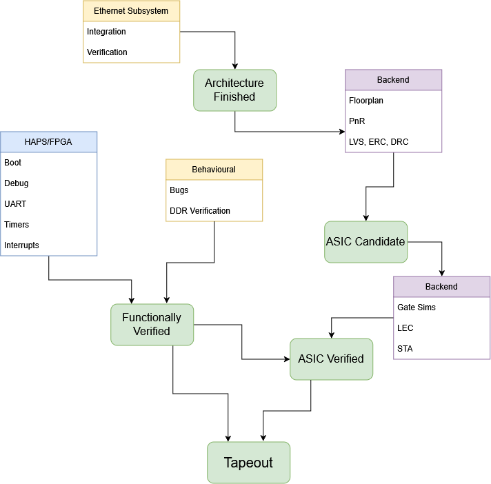
The current status of the project is shown above. The SoC architecture is almost completely finished. However, with the recent tapeout of the nanoSoC ethernet chiplet providing an alternate ethernet IP solution, we are aiming to add this IP into megaSoC V1. This which will require integration, and verification. Backend ASIC work has begun. This has been started without the full SoC being finalised. This is to ensure that when final RTL is frozen, the necessary scripts are already in place to allow for a smooth tapeout process.
The full verification of the SoC is still underway. One gating item is getting the SoC implemented into FPGA/HAPS to ensure that we have all the functionality we need for a linux OS to boot. Namely these are UART, timers interrupt and a boot process. The main IP that is yet to be fully verified via system integration is the JTAG debugger access port to the Cortex A53, which is often much simpler to verify when instantiated in FPGA. Once fully verified, the final backend can be run, and then verified against gate simulations, LEC, STA, as well as DRC, LVS, and ERC to ensure proper ASIC functionality.
Project Milestones
Do you want to view information on how to complete the work stage ""
or update the work stage for this project?
-
Architectural Design
Design FlowTarget DateCompleted DateOverall architecture of megaSoC
Result of WorkThe overall architecture is complete for this and can see from the architectural diagram.
-
Clock Tree Synthesis
Design FlowTarget Date -
Design for Test
Design FlowTarget DateIn this complex SoC we have yet to decide exactly what scheme we will use for DFT.
This is a point that needs further clarification/discussion in the team
-
Logical verification
Design FlowTarget DateLogical equivalence checking and gate level simulations will be needed.
For a SoC of this size, gate level simulations may be impractical, but are usually good to check bootup sequence at the very least
-
Routing
Design FlowTarget Date -
Behavioural Design
Design FlowTarget Date~90% complete. Core SoC interconnect fully integrated. Expansion region is an intentional stub for user accelerators.
- **Remaining work**: Bug fixes from simulation, any final integration tweaks. Ethernet/PTP integration
-
Physical Verification
Design FlowTarget DateFull DRC, STA, and LEC should be complete on this design.
Initial DRC will be complete before 30th June 2026, as that is when we have to register for the tapeout slot. Ideally at this point we will have some idea on how realistic an october tapeout will be
-
RTL Verification
Design FlowTarget DateVerification of the system is ongoing. Most of the subsystems/IP are pre-verified. So only integration verification is needed. Parts still to be verified are:
- DDR controller
- SDIO controller
- Reset controller
Furhter verification tests are needed, We are working on the verification methodology using AI assisted verification
-
Synthesis
Design FlowTarget DateInitial synthesis of the Cortex A53 is near completion.
The rest of the SoC is still to go. The plan for this is to do a hierarchical approach, so the Cortex A53 and DRAM controller will be synthesised seperately, then integrated into the full system.
Update 13/07/2026 - Scripts in place (FusionCompiler). QSPI partition completed clean signoff on TSMC 65nm. A53 initial synthesis "near completion." No completed full-SoC runs. Library setup (TSMC 16nm cln16fcll) complete
Remaining: Hierarchical approach — synthesise A53 and DRAM controller separately, then full SoC. Run initial synthesis, iterate on timing.
-
Floor Planning
Design FlowTarget DateAs we are planning on using Synopsys Fusion Compiler for the backend, floorplanning and synthesis will happen simultaneously.
The hierarchical approach will mean treating the Cortex A53 and DDR controller as macro blocks.
Some time will be allocated for floorplan exploration as well
-
Tape Out
Design FlowTarget DateInitial (ambitious) deadline for tapeout on europractise MPW for TSMC 16nm
-
Getting Started
Design FlowCompleted DateResult of WorkEnvironment already setup for this project in the SoCLabs server
-
Specifying a SoC
Design FlowCompleted DateResult of WorkThe aims for the SoC is to build a linux capable system. This will be achieved using an application class processor (A53) with filesystem storage (SD card), and system memory (LPDDR4). The networking for this initial version of the SoC will be performed using SLIP (serial line internet protocol) over UART.
-
IP Selection
Design FlowCompleted DateResult of WorkThe SoC consists of:
- Arm Cortex A53
- Arm GIC-400
- Arm PCK-600
- Arm NIC-400
- SoCLabs QSPI AHB controller
- Arm Corstone 101
- Arm PL011
- Open source SDIO controller (from ZipCPU)
- Synopsys uMCTL2 DDR controller and LPDDR4 multiPHY
-
Technology Selection
Design FlowCompleted DateResult of WorkAim for this project is to tape out with Europractise on the TSMC 16nm MPW

Team



 Project Creator
 Daniel Newbrook
Digital Design Engineer
at University of Southampton
Research area: IoT Devices
ORCID Profile
 Cortex-A53
 CoreLink NIC-400
 Corelink DMA-350
 PCK-600 Power Control Kit
 GIC-400 General Interrupt Controller
 Hardware design
Submitted on
Comments
Synthesis milestone
Hi,
When did we say "Initial synthesis of the Cortex A53 is near completion" and in retrospect how complete was it?
Missing info on Behavioural Design milestone
Hi,
Looking at this milestone:
It is not clear when we started it and when we were at 90%?
Add new comment
To post a comment on this article, please log in to your account. New users can create an account.